


-
随着加速器粒子物理实验的发展,探测器朝着高位置分辨率、高精度能量分辨以及快时间响应的方向发展。电子学处理的信号变快,通道数随之剧烈增加,因此对电子学提出了高集成度和数字化前移等需求,使得在读出电子学前端基于专用集成电路(Application Specific Integrated Circuit, ASIC)实现模拟信号调理、信号数字化以及数据汇总成为读出电子学发展的一个趋势。但这也使得ASIC暴露在高能粒子辐照环境中,对电子学芯片的抗辐照性能提出了严苛的要求。其中静态随机存储器(Static Random-Access Memory, SRAM)是ASIC中一个非常重要的组成部分。例如在ATLAS探测器中用于前端数据汇总的ROC芯片使用了大量的基于SRAM的FIFO进行数据的暂存和缓冲[1]。此外在硅像素探测器的读出电子学中,基于低功耗小面积的考虑,阈值调节部分也通常采用SRAM控制一个数模转换器(Digital-to-Analog Converter, DAC)来实现[2]。然而SRAM在辐射环境中容易发生单粒子翻转(Single Event Upset, SEU),从而给芯片使用带来严重的问题[3]。SEU是指当高能粒子撞击SRAM单元敏感节点时,粒子的能量将会沿着其穿过的路径沉积在半导体材料中,并产生电子空穴对,这些电子空穴对在电场的漂移作用下被有效地收集到敏感节点处,造成电荷的积累,产生瞬态电流脉冲。当粒子的能量足够大,产生的电子空穴对足够多时,SRAM中存储单元的逻辑值将会发生改变,造成单粒子翻转[4]。并且随着CMOS晶体管的尺寸不断缩小,SRAM发生SEU的概率也随之增大。因此很多研究机构都进行了SRAM单元抗SEU的研究。1988年IBM公司曾提出通过节点冗余加反馈的方法来实现SRAM存储单元逻辑值不被高能粒子破坏,当逻辑值被粒子撞击而发生翻转时,通过反馈可以将被翻转的数据恢复[5]。1996年Calin等[6]提出了一种非常经典的12个晶体管的双锁存单元(DICE)结构,也是使用了节点冗余加反馈的方法来进行SRAM抗SEU加固。2016年的一篇文章[7]提出的一种12个晶体管的抗SEU单元,也是通过上述方法来实现加固。2020年Haran等[8]提出了一种工作于亚阈值电压下的13管单元结构,通过节点反馈来抗SEU加固。通过增加额外的晶体管进行节点冗余备份的方法,其逻辑值不由单一反馈路径决定,因此单个粒子撞击仅仅在单个敏感节点产生瞬态电流不会造成其翻转,所以它具有良好的抗SEU的性能。然而,节点备份这种方法需要更多的存储节点和电源到地的支路,在写入数据时需要翻转的节点数量也会随之增加,因此其功耗亦会增大。
此外,2006年Sasaki等[9]提出了一种基于施密特电路的寄存器单元用来掩蔽组合电路上的瞬态脉冲造成的软错误。2009年Sheng 等[10]提出了两种基于施密特结构的锁存器以提高锁存器对软错误的容忍度。2015年Rajaei等[11]提出了一种具有13个晶体管的SRAM单元,其基于施密特触发器电路和反相器互锁的结构通过提高SRAM单元的翻转阈值来实现抗SEU加固。此外文献[12-16]也对将施密特触发器应用于锁存单元或SRAM单元进行了研究。
本论文根据对上述论文的分析和研究提出了一种由11个晶体管组成的SRAM单元结构,其基于施密特触发器的工作原理通过提高SRAM单元的翻转阈值,使其拥有更高的静态噪声容限,以此来实现SEU加固。并且采用额外的控制信号在写操作时断开反馈,以减小功耗。
-
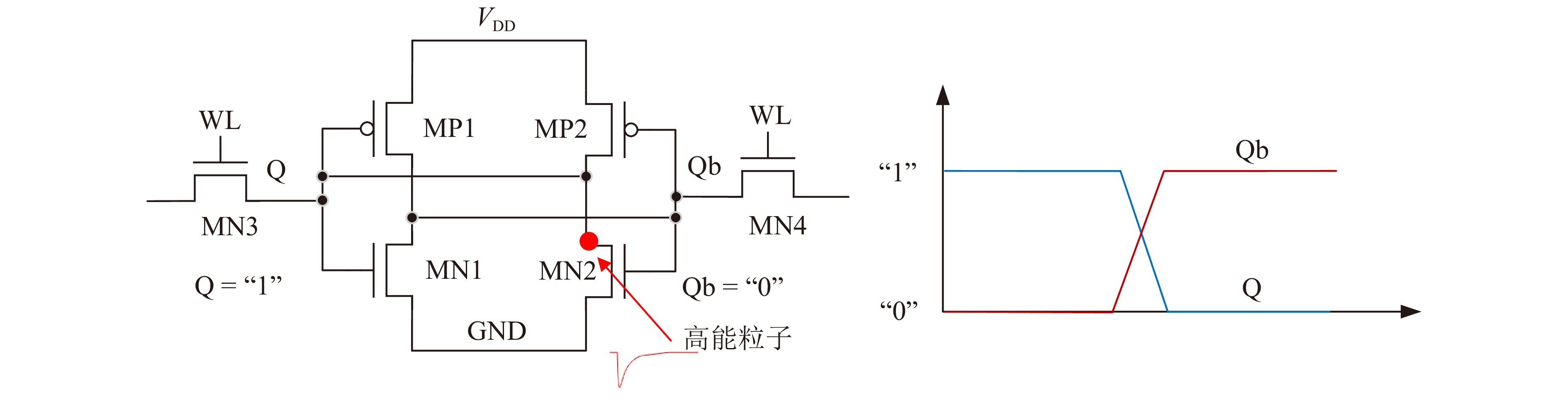
普通的6管SRAM单元结构由两个反相器互锁组成,另由两个晶体管作为存取管,如图1所示。当高能粒子轰击器件时,沿着粒子轨迹将产生大量的电子空穴对。在电场的作用下这些电子和空穴沿相反的方向移动,被不同的电极收集,产生瞬态电流。因此当高能粒子击中SRAM中的敏感节点Q或者Qb,且敏感节点上积累的瞬态电荷量足够大时, SRAM将会发生单粒子翻转,如图1所示。

图 1 SRAM 6管单元电路单粒子翻转示意图(在线彩图)
-
基于传统施密特触发器结构设计的12管SRAM单元电路如图2所示,由一个反向器和一个传统施密特触发器结构的反向器互锁组成[10]。该结构采用的传统的施密特触发器结构如图3(a)电路所示,该电路具有迟滞性[17]。当施密特触发器输入电压高于正向阈值电压,输出为低;当输入电压低于负向阈值电压,输出为高;当输入在正负向阈值电压之间,输出不改变。而12管SRAM单元即通过施密特触发器的迟滞性提高SRAM单元的翻转阈值来实现SEU加固。图3(b)所示施密特触发器电路为本论文中使用的结构,其原理和传统的施密特触发器电路原理相似,即通过额外电路改变MN2和MP2的源极电压,来达到迟滞的效果。并且相对于传统的施密特触发器电路,该结构,在输入电压在从0到1 (从1到0)变化时,不会出现电源通过导通的MN3和MN1(MP3和MP1)到地的情况,因此功耗更低。

图 2 基于施密特触发器的12管SRAM结构[10]

图 3 施密特触发器电路结构
-
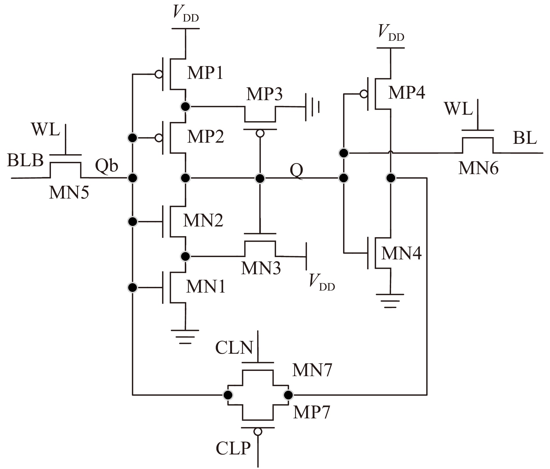
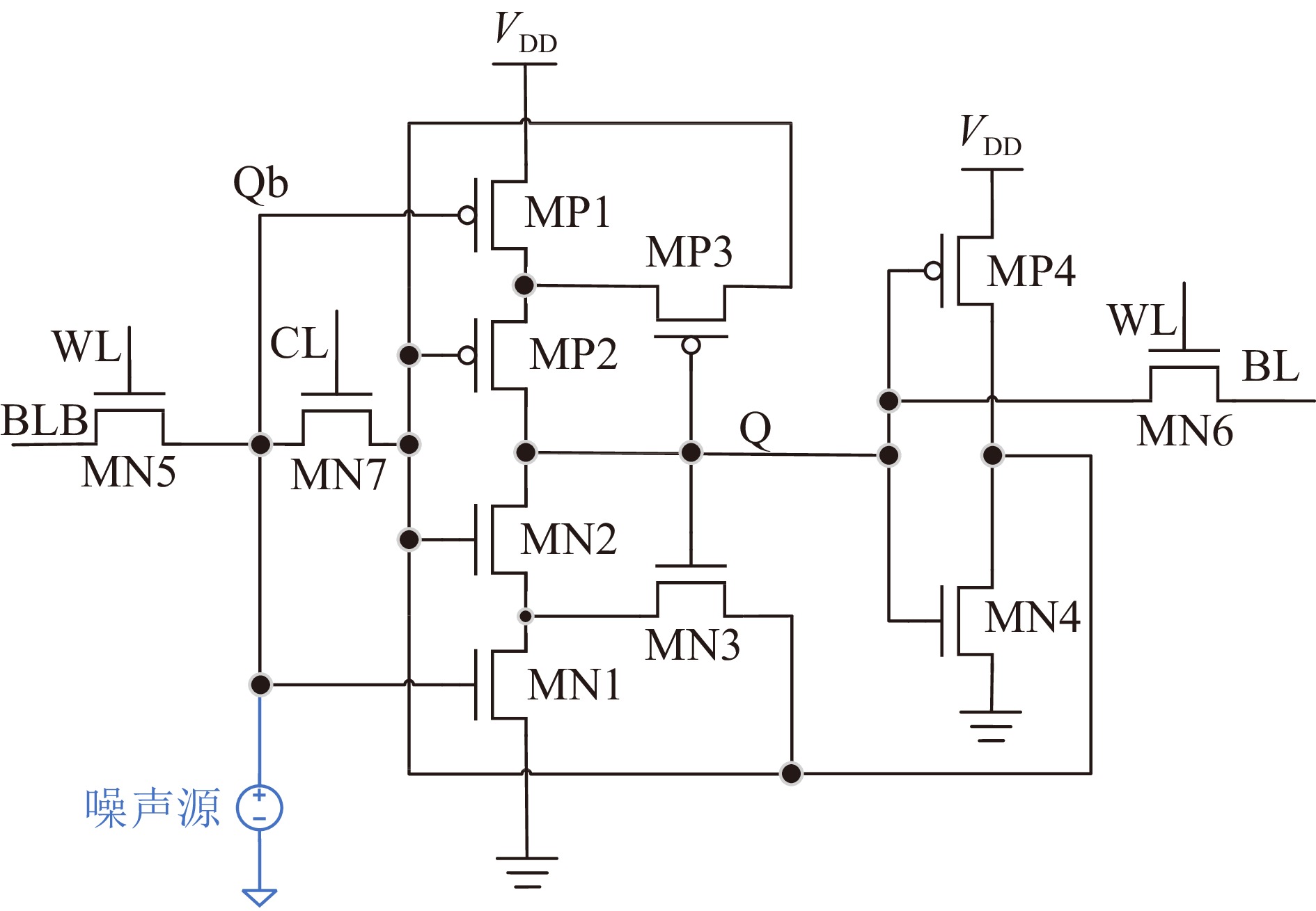
本文提出的改进型基于施密特触发器结构的11管SRAM单元电路如图4所示。该单元电路由4个PMOS管MP1~MP4以及7个NMOS管MN1~MN7组成。这些MOS管构成一个反向器和一个基于施密特触发器结构的反相器互锁连接,提供Q和Qb两个互锁的节点来进行数据存储。其中PMOS管MP1,MP2,MP3和NMOS管MN1,MN2,MN3组成基于施密特触发器的反相器。PMOS管MP4和NMOS管MN4组成一个普通的反相器。基于施密特触发器反相器的输出连接到普通反向器的输入,普通反向器的输出连接到基于施密特触发器反相器的输入。此外11管单元中的MP3管的漏极和MN3管的漏极接在基于施密特触发器结构的反相器的输入端。

图 4 基于施密特触发器的SRAM 11管单元结构
-
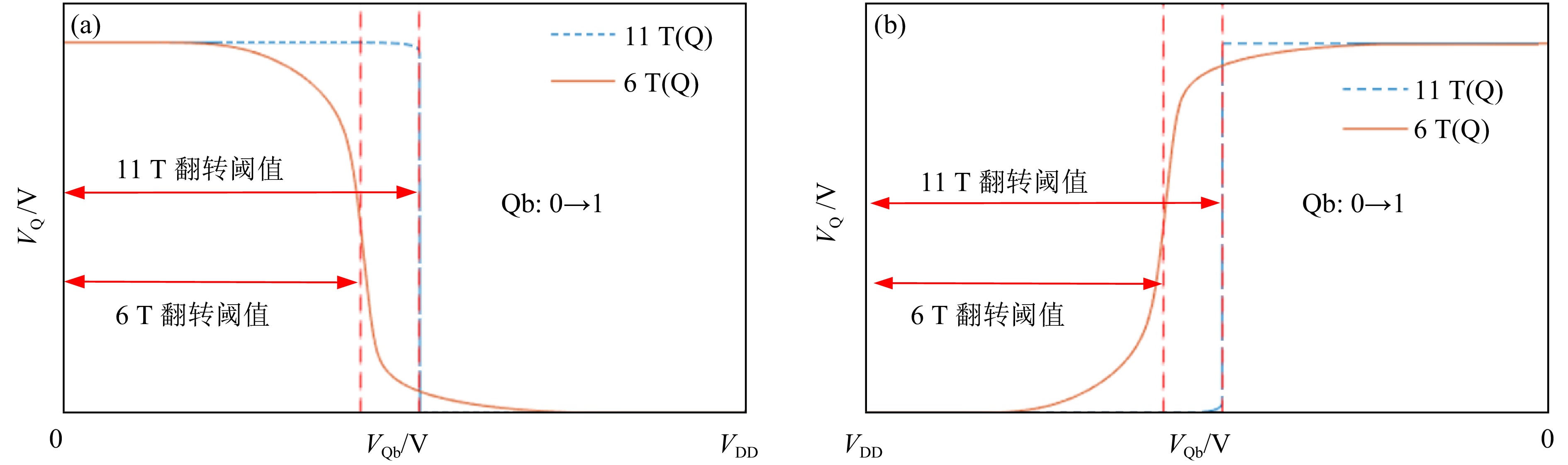
在11管单元中,当Qb为0,Q为1时,MN3导通,其漏极接到Qb节点,MN1源极电压将会随着Qb的变化而变化,而MP3截止。当高能粒子轰击敏感节点Qb 使其电压VQb发生改变。当VQb小于MN1管的阈值电压时,MN1不会导通,电路也不会发生翻转。当VQb逐渐升高大于MN1管的阈值电压时,由于MN3管导通,MN2的源极电压跟随VQb变化,所以MN2的栅源电压小于其阈值电压,MN2依然截止。随着VQb的不断升高迫使MP1和MP2的栅源电压变小,导通电阻增加,从而导致Q点电位下降,进而使得MN3管的导通电阻增大。当Q点电位低到使MN3管关断时,MN2的源极电压将不在跟随Qb变化,进而导致MN2的栅源电压大于其阈值电压,MN2导通。电路此时才开始发生翻转。因此从Qb到Q的翻转阈值增大,从而使得SRAM翻转所需电荷增加,以此来实现SEU加固,如图5(a)所示。当Qb为1,Q为0时,原理同上,如图5(b)所示。并且由于11管单元中的MP3管的漏极和MN3管的漏极接在基于施密特触发器结构的反相器的输入端,高能粒子轰击敏感节点Qb产生的瞬态电流可以通过MN1、MN3或MP1、MP3释放掉一部分,因此可以进一步增加Qb节点的抗SEU能力。当高能粒子轰击Q点时,由于此节点有较大的寄生电容,虽然此节点的翻转阈值没有较大的提高,但依然可以依靠相对大的寄生电容来进行SEU加固。

图 5 11管单元与6管单元翻转阈值示意图(在线彩图)
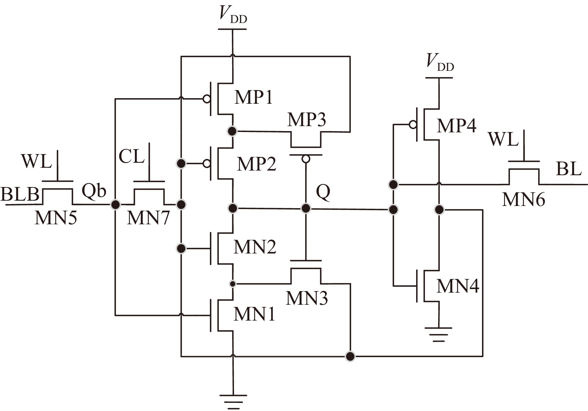
此外存取管MN5和MN6由WL控制。这里为了降低写功耗还增加了一个NMOS管MN7,用来隔离MP1和MN1的栅极和Qb之间的连接,MN7由CL控制。在保持状态时CL为1,WL为0,此时基于施密特触发器反相器与反向器互锁,使数据保持不变。在写操作时CL为0,断开反相器间的反馈,降低写功耗。
-
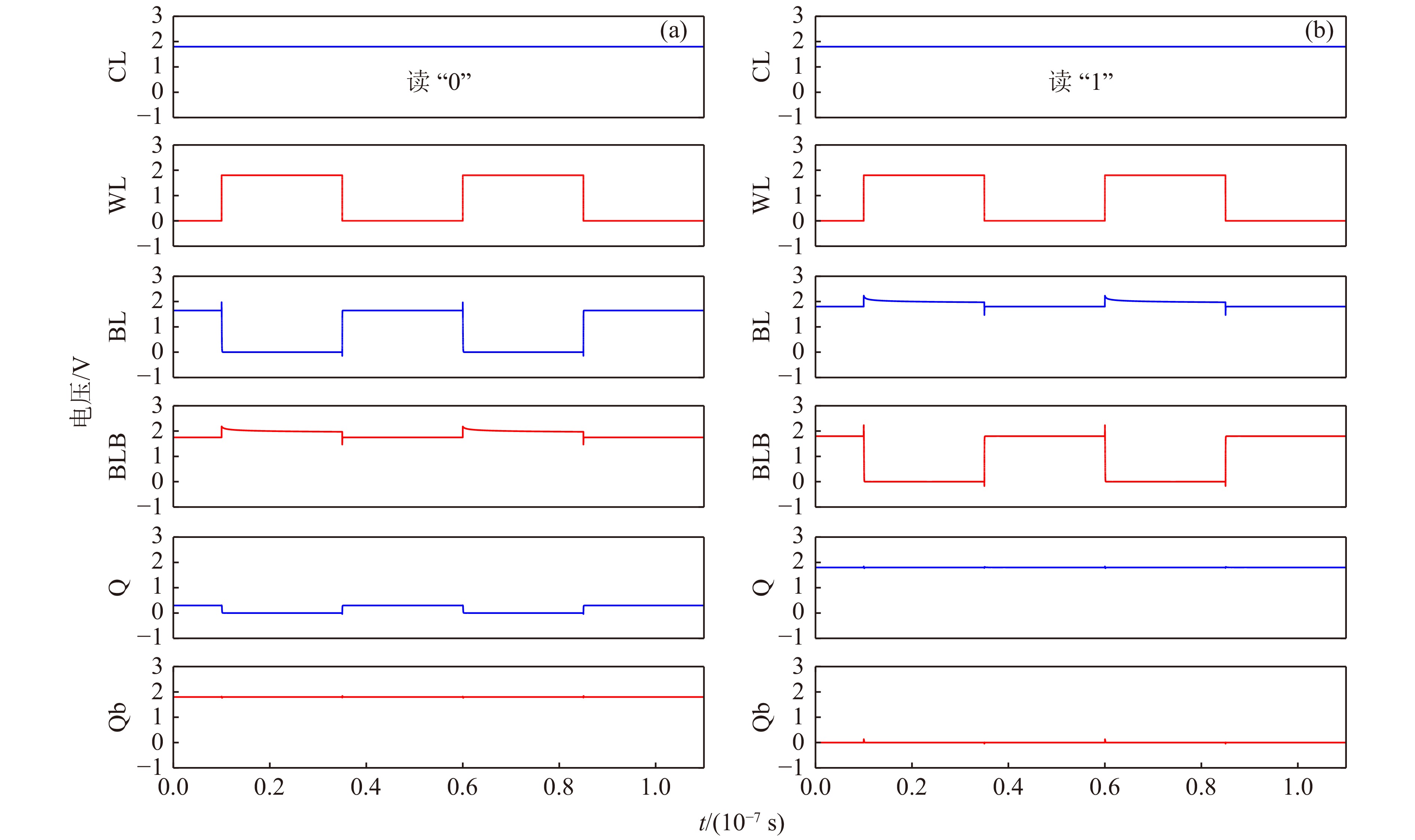
在读操作之前,先将位线BL与互补位线BLB预充到高电平,同时字线WL保持在低电平,而控制线CL保持在高电平。假设此时单元存储的逻辑值为1,则节点Q为高电平,Qb为低电平。当读取操作开始时,保持CL为高电平不变,升高WL的电压,使得存取管MN5和MN6打开。此时由于Q点为高电平,所以BL上的电压几乎保持不变。由于Qb为低电平,BLB线会被缓慢放电,直到BL与BLB的电压差可以被灵敏放大器检测。对于读操作其与普通六管单元无异。图6展示了11管单元读操作波形图。

图 6 11管单元读操作波形图(在线彩图)
-
对于写操作,假设单元在写操作执行之前存储的逻辑值为0,即节点Q为低电平,Qb为高电平,并且要将逻辑1写入。因此先将BL置为高电平,BLB置为低电平,并且将CL置为低电平,此时反向器到MN1和MP1的栅极连接被断开,BLB通过存取管MN5连接到MN1和MP1的栅极,MN1和MP1的栅极呈现高阻态且其电压由于寄生电容的作用依旧为高。升高WL的电压使得存取管MN5和MN6打开。此时由于MN1和MP1的栅极只通过存取管MN5与BLB相连,MN1和MP1的栅极的电压变为低,Q点到地的通路被断开。又由于Q点通过MN6管与BL相连,则Q点电压很快被充电到高电平。
当Q点被充电到高电平时,经过由MP4和MN4组成的反向器,Qb点电压被放电到低电平。当WL变为低,CL变为高,写操作结束,单元存储数据由逻辑0写为逻辑1,普通反向器和基于施密特触发器的反向器形成互锁数据得以保存。图7展示了11管单元写操作波形图。

图 7 11管单元写操作波形图(在线彩图)
-
采用180 nm 标准商用CMOS工艺在Cadence virtuoso中设计了上述11管单元结构的原理图,并对其进行了噪声容限仿真、SEU仿真和功耗仿真。
-
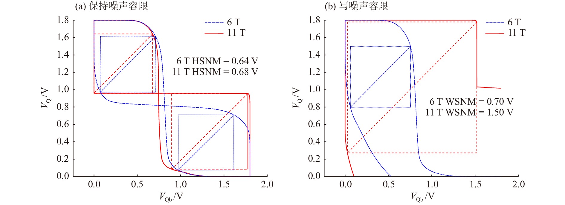
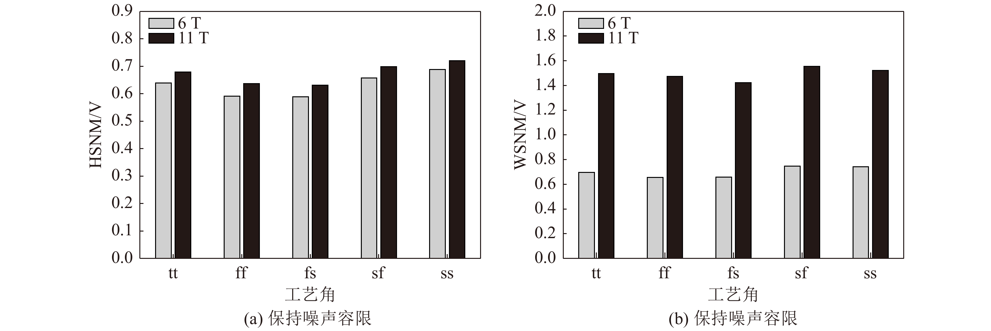
静态噪声容限(SNM)经常被用来衡量SRAM单元的稳定性,特别是写和保持条件下的静态噪声容限[18]。SNM的仿真方法如图8所示,通过在敏感节点插入单端噪声源,来观察Q和Qb节点的电压。经过仿真得到的普通6管单元和11管单元的保持静态噪声容限(HSNM)和写静态噪声容限(WSNM)如图9所示,图中虚线正方形的对角线的长度为SNM的大小。在电源电压1.8 V、tt工艺角和25 ºC条件下,仿真结果表明,11管单元的HSNM为0.68 V,相比6管单元的0.63 V提升了6%。在此条件下,11管单元的WSNM为1.50 V,相比于6管单元的0.70 V有两倍以上的提升。图10展示了在通用NP(tt)、快N快P(ff)、快N慢P(fs)、慢N快P(sf)和慢N慢P(ss)等5种不同工艺角下上述噪声容限仿真结果,可以看到在不同的工艺角下11管单元相比6管单元都有提升,且写噪声容限提升明显。

图 8 11管结构SNM仿真原理图(在线彩图)

图 9 普通6管单元和11管单元SNM (在线彩图)

图 10 不同工艺角下普通6管单元和11管单元的SNM (在线彩图)
-
为了验证本论文中SRAM单元的抗SEU性能,仿真是必不可少的。这里使用文献[19]中提出的双指数电流注入模型来模拟粒子轰击在器件上所产生的瞬态电流。
$$ \begin{split} \\ I(t) = {\text{ }}{I_0}({{{\rm{e}}}^{ - \alpha t}} - {{{\rm{e}}}^{ - \beta t}}) \text{,} \end{split}$$ (1) 式中:
$ {I_0} $ 为注入电流的大小;$ \alpha $ 和$ \beta $ 为时间常数。对该电流源积分即可得到该节点的注入电荷。由上文可知SRAM单元被高能粒子轰击敏感节点时会沉积大量的电荷,当沉积的电荷足够多时该节点将会发生翻转,而产生翻转所需的最小电荷量叫做临界电荷
$ {Q_{{\text{Cri}}}} $ 。当模拟一个高能粒子轰击敏感节点时,将一个双指数电流源连接到该节点,通过仿真可以得到不同的注入电荷对SRAM敏感节点的影响,并且找到该敏感节点的临界电荷。此外本电路设计采用的CMOS工艺其衬底材料为硅,通过式(2)可以计算出敏感节点收集到的电荷$ {Q_{\text{C}}} $ 对应的粒子LET值[20]:$$ {Q_{C}} = 1.03 \times {10^{ - 2}}{\text{ }}({L_{{\rm th}}} {\boldsymbol{\cdot}} T)\;{{\rm{pC}}} \text{,} $$ (2) 这里
$ {Q_C} $ 的单位是pC;${L_{{\rm th}}}$ 的单位是$ \text{MeV}\cdot \text{c}{\text{m}}^{\text{2}}\text{/mg} $ ;$ T $ 的单位为μm。将双指数电流脉冲在保持状态下注入到11管单元的敏感节点中,其仿真波形如图11所示。表1显示了普通6管单元、11管单元和12管单元各节点临界电荷仿真结果。11管单元相比于6管单元和12管单元造成单粒子翻转所需的临界电荷都有明显提升,并且从1到0翻转和从0到1翻转所需临界电荷有差异。且11管单元是非对称的Q与Qb节点的临界电荷亦不相同。

图 11 SEU仿真波形图(在线彩图)
表 1 SEU仿真结果对比表
节点 翻转 临界电荷/fC LET(MeV·cm2/mg)器件厚度2 μm 6管 Q/Qb 0→1 223.8 10.86 1→0 180.4 8.76 11管 Q 0→1 286.2 13.89 1→0 224.2 10.88 Qb 0→1 1 328.3 64.48 1→0 794.5 38.57 12管 Q 0→1 273.1 13.25 1→0 218.1 10.58 Qb 0→1 891.2 43.26 1→0 509.1 24.71 -
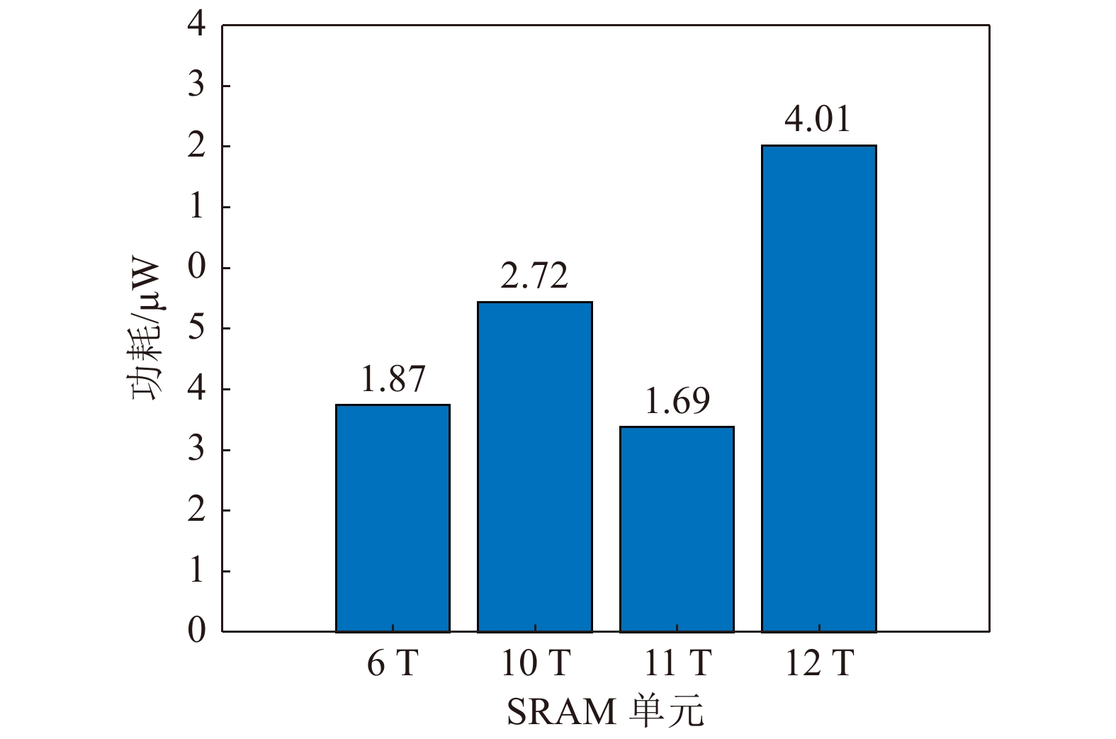
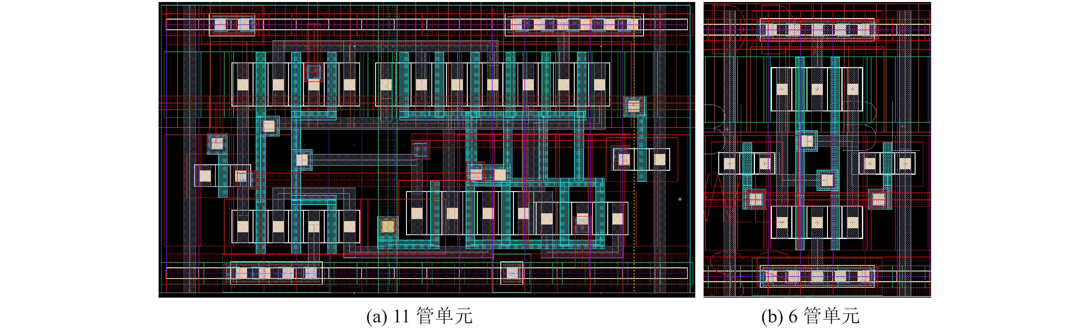
在工作电压为1.8 V,工作频率20 MHz下仿真6管单元、11管单元、将11管单元中MN7管去掉后的10管单元及12管单元的平均功耗,如图12所示。由于11管单元在写操作时会先断开反馈,所以可以看到,加入MN7管后11管单元的功耗节省了37%。并且由于在写0操作过程中12管单元存在电源通过MP1和MP3到地导通的情况,12管单元的功耗是11管单元的2.4倍。图13为11管单元和普通6管单元的版图,其中普通6管单元的面积为4.62 μm ×5.04 μm,11管单元的面积为10.56 μm×5.04 μm。

图 12 不同SRAM单元功耗对比图(在线彩图)

图 13 11管单元和普通6管单元版图(在线彩图)
-
在本论文中提出了一种基于施密特触发器结构的的11管SRAM单元,并基于180 nm CMOS工艺进行了电路设计和仿真。仿真结果表明,该11管SRAM单元相比于普通6管SRAM单元具有更强的抗SEU能力,在敏感节点Q最差情况相比于6管SRAM单元其临界电荷增加了1.24倍,而在敏感节点Qb最差情况相比于6管SRAM单元其临界电荷增加了4.40倍。相比于12管SRAM单元,在敏感节点Q临界电荷增相差不大,而在敏感节点Qb最差情况相比于12管SRAM单元临界电荷增加了1.56倍。
-
摘要: 在加速器粒子物理实验中,基于专用集成电路(Application Specific Integrated Circuit, ASIC)在读出电子学前端实现模拟信号调理、数字化等功能是一个发展趋势,但这也使得ASIC暴露在了高能粒子辐射环境中,而其中的静态随机存储器(Static Random-Access Memory, SRAM)容易受到辐射的影响产生单粒子翻转(Single Event Upset, SEU),从而使芯片工作异常。因此对ASIC中的SRAM进行抗辐照加固设计十分必要。本工作提出了一种基于施密特触发器结构的11管抗SEU SRAM存储单元,并在180 nm CMOS工艺下进行了电路的设计和仿真,仿真结果表明,与传统12管SRAM单元相比,抗单粒子翻转能力有明显增加,且功耗仅为12管单元的42%。Abstract: In accelerator particle physics experiments, it is a development trend to realize the functions of analog signal processing and digitization at the front end of readout electronics based on application specific integrated circuits(ASICs), but it also exposes ASICs in the radiation environment of high-energy particles, The static random access memory(SRAM) is vulnerable to radiation, resulting in single event upset(SEU), which makes the chip abnormal. Therefore, it is necessary to design radiation-hardened SRAM in those ASICs. In this paper, a SEU-tolerant SRAM memory cell with 11 transistors(11 T) based on Schmitt trigger is proposed. The circuit is designed and simulated in 180 nm CMOS process. The simulation results show that our proposed 11 T SRAM cells as compared with traditional 12 transistors(12 T) SRAM cell have considerably higher robustness against single-event multiple effects, and consumes only 42% power of the 12 T cell.
-
Key words:
- SRAM cell /
- SEU /
- ASIC /
- radiation resistance
-
图 8 11管结构SNM仿真原理图(在线彩图)
HSNM时BL/BLB为高电平,WL为低电平存储节点Q/Qb一个高一个低存储数据;HSNM时WL选中为高电平,BL Qb/BLB Q一个为高一个为低。
表 1 SEU仿真结果对比表
节点 翻转 临界电荷/fC LET(MeV·cm2/mg)器件厚度2 μm 6管 Q/Qb 0→1 223.8 10.86 1→0 180.4 8.76 11管 Q 0→1 286.2 13.89 1→0 224.2 10.88 Qb 0→1 1 328.3 64.48 1→0 794.5 38.57 12管 Q 0→1 273.1 13.25 1→0 218.1 10.58 Qb 0→1 891.2 43.26 1→0 509.1 24.71  下载: 导出CSV
-
[1] COLIBAN R M, POPA S, TULBURE T, et al. Journal of Instrumentation, 2016, 11(02): C02069. doi: 10.1088/1748-0221/11/02/c02069 [2] GAO C, HUANG G, SUN X, et al. Journal of Instrumentation, 2016, 11(01): C01053. doi: 10.1088/1748-0221/11/01/c01053 [3] BARAK J, YITZHAK N M. IEEE Transactions on Nuclear Science, 2015, 62(6): 3369. doi: 10.1109/TNS.2015.2495324 [4] MESSENGER G C, ASH M S. Single Event Phenomena[M]. New York: Springer US, 1997: 15. [5] ROCKETT L. IEEE Transactions on Nuclear Science, 1988, 35(6): 1682. doi: 10.1109/23.25522 [6] CALIN T, NICOLAIDIS M. IEEE Transactions on Nuclear Science, 1996, 43(6): 2874. doi: 10.1109/23.556880 [7] QI C, XIAO L, WANG T, et al. IEEE Transactions on Device & Materials Reliability, 2016, 16(3): 388. doi: 10.1109/TDMR.2016.2593590 [8] HARAN A, KEREN E, D DAVID, et al. IEEE Transactions on Nuclear Science, 2020(99): 1. doi: 10.1109/TNS.2020.3002654 [9] SASAKI Y , NAMBA K , ITO H . Soft Error Masking Circuit and Latch Using Schmitt Trigger Circuit[C]//21st IEEE International Symposium on Defect and Fault Tolerance in VLSI Systems, October 04-06, 2006, Arlington, VA, USA. New York: IEEE, 2006: 327. [10] SHENG L, KIM Y B, LOMBARDI F. Soft-Error Hardening Designs of Nanoscale CMOS Latches[C]// 27th IEEE VLSI Test Symposium, May 03-07, 2009, Santa Cruz, CA, USA. New York: IEEE, 2009: 41. [11] RAJAEI R, ASGARI B, TABANDEH M, et al. IEEE Transactions on Device and Materials Reliability, 2015, 15(99): 429. doi: 10.1109/TDMR.2015.2456832 [12] SHENG L, KIM Y B, LOMBARDI F. IEEE Transactions on Device & Materials Reliability, 2012, 12(1): 68. doi: 10.1109/TDMR.2011.2167233 [13] GLORIEUX M, CLERC S , GASIOT G, et al. IEEE Transactions on Nuclear Science, 2013, 60(6 Part1): 4381. doi: 10.1109/TNS.2013.2284604 [14] JIANG H, ZHANG H, BALL D R, et al. SE performance of a Schmitt-trigger-based D-flip-flop Design in a 16-nm Bulk FinFET CMOS Process[C]// /2016 IEEE International Reliability Physics Symposium (IRPS), April 17-21, 2016, Pasadena, CA, USA. New York: IEEE, 2016. 3B-2-1. [15] YAN A, HU Y, SONG J, et al. Single-Event Double-Upset Self-Recoverable and Single-Event Transient Pulse Filterable Latch Design for Low Power Applications[C]//Design, Automation & Test in Europe Conference & Exhibition (DATE), March 25-29, 2019, Florence, Italy. New York: IEEE, 2019: 1679. [16] LI Y, CHENG X, TAN C, et al. AIEEE Transactions on Circuits and Systems II: Express Briefs, 2020, 67(9): 1619. doi: 10.1109/TCSII.2020.3013338 [17] SCHMITT O H. Journal of Scientific Instruments, 1938, 15(1): 24. doi: 10.1088/0950-7671/15/1/305 [18] LIST F J. The Static Noise Margin of SRAM Cells[C]// European Solid-state Circuits Conference. New York: IEEE Xplore, 1986. [19] MESSENGER G C. IEEE Transactions on Nuclear Science, 1983, 29(6): 2024. doi: 10.1109/TNS.1982.4336490 [20] MENDENHALL M. Critical Charge and Threshold LET[EB/OL]. [2022-01-15]. https://creme.isde.vanderbilt.edu/CREME-MC/help/critical-charge-and-threshold-let.htm. -

 点击查看大图
图(13) / 表 (1)
计量
- 文章访问数: 638
- HTML全文浏览量: 198
- PDF下载量: 73
- 被引次数: 0


 甘公网安备 62010202000723号