


 下载:
下载:


-
近年来,物理实验,尤其是粒子物理实验和核物理实验,朝着大规模化方向发展,因此需要其数据传输系统具备高速且稳定的特点。一般来讲,数据传输方式主要分为并行传输和串行传输两种方式。随着通信速率不断提高,串行数据传输模式成为了主流的通信方式。
并串行与串并行转换器SERDES (SERializer / DESerializer)[1]在发送端将多路低速并行信号转换成高速串行信号,在接收端将高速串行信号重新转换成低速并行信号。由于SERDES具有传输速度快、可靠性高、连接简单的技术优势,使其成为物理实验装置中高速串行数据传输的理想选择,因此国内外科研机构开展了大量的研究, 其中比较有代表性的主要包括ATLAS Liquid Argon Calorimeter的LOCx2芯片[2]、LHC的GBTx芯片[3]、HL-LHC的IpGBT芯片[4]、南方卫理公会大学研发的基于PAM4编码的20 Gbps SERDES[5]等。
为了满足物理实验数据传输芯片国产化的需求,本课题组基于国内GSMC 130 nm工艺设计了一款5 Gbps的SERDES芯片,其中20:1的并串转换电路(Serializer)用于将20路250 Mbps并行数据转换成1路5 Gbps的高速串行数据,是SERDES芯片的核心电路模块。下面将从总体结构设计、各模块设计和版图设计及仿真验证来介绍该Serializer电路模块的设计。
-
并串转换电路常用结构主要有并行结构、串行结构和树型结构[6]。并行结构由一个多相时钟发生器产生时钟信号并对每路并行输入数据进行选择,依次控制多路选通器输出一路被选通的数据,并行结构适用于输入数据位宽较少的高速转换系统,该结构要求时钟和数据具有较高的相位匹配关系。串行结构通过移位寄存器串联而成,结构简单,但需要所有寄存器都工作在输入数据的速率上,适用于中低速情况。而树型结构,其所需驱动时钟频率仅为最大串行数据率的一半,采用分级解串降速的方式使得电路获得较高速率同时兼具低功耗的优点,因此在高速转换情况下常用到树型结构[7]。
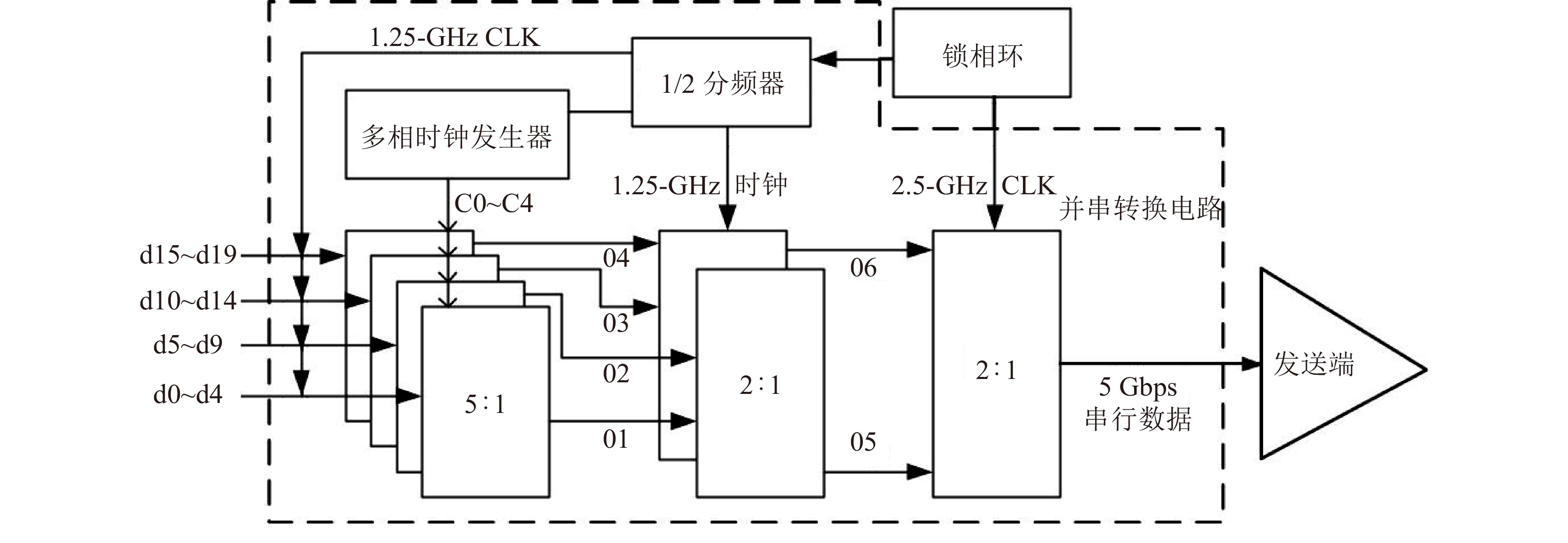
针对20路并行数据输入的要求,本文利用常用结构的优点,采用并行结构和树型结构相结合的方式,设计了一款多路选择开关式的并串转换电路。本文并串转换电路整体结构如图1所示,它由三级并串转换模块串联而成。其中第一级由4个5:1并转串模块并行构成,第二、三级则是树型结构的2:1并转串模块。在第一级中,并行的20路250 Mbps的输入数据d0~d19被分成4组,每组5路数据输入到5:1并转串模块转换成串行数据输出,从而形成4路1.25 Gbps的数据O1~O4。这四路数据经过第二级2个2:1并转串模块输出两路2.5 Gbps数据,再经过第三级的2:1并转串模块,最终输出1路5 Gbps高速串行数据。这三级并串转换模块所需的时钟总信号来自片内2.5 GHz锁相环(Phase Lock Loop, PLL),其中第二、三级树型结构的2:1并转串模块,它们所需的时钟信号分别来自二分频器生成的1.25 GHz时钟信号和PLL提供的2.5 GHz时钟信号,而第一级5:1并转串模块是并行结构,其所需时钟信号由多相时钟发生器(Finite State Machine, FSM)提供,FSM生成5种(C0~C4)不同相位的1.25 GHz时钟信号用于控制5:1并转串模块。
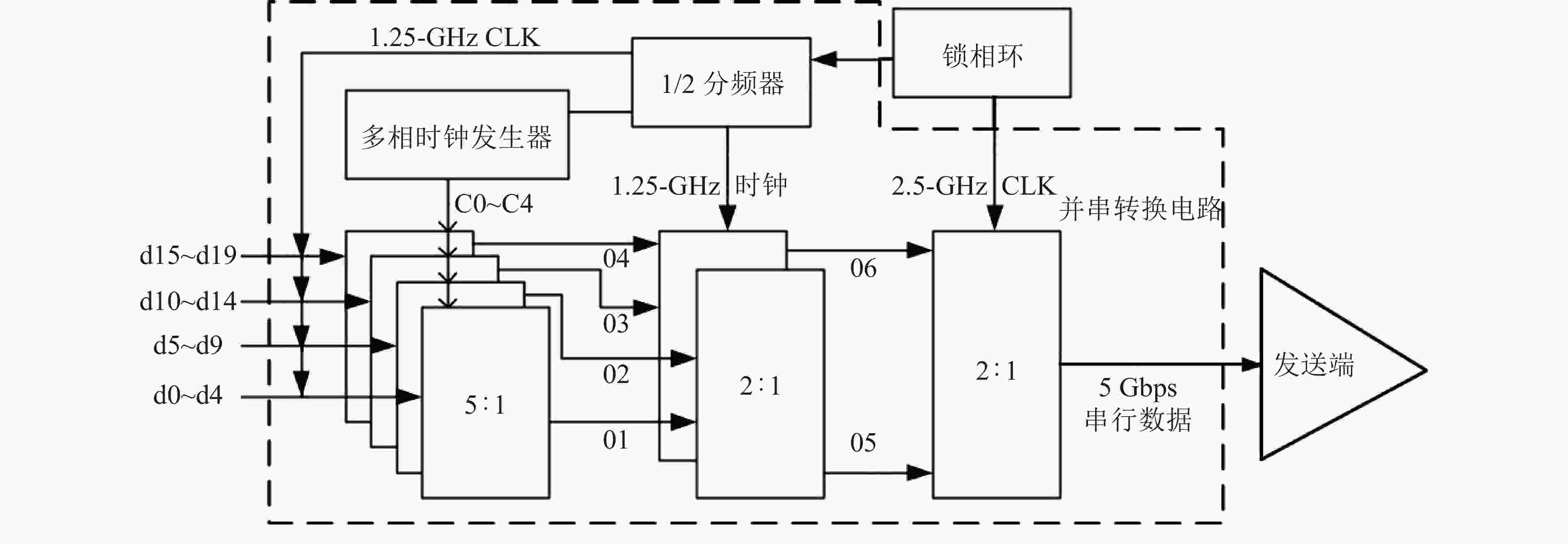
图 1 并串转换电路整体结构
-
并串转换器芯片第一级由多相时钟发生器和4个5:1并转串模块组成。多相时钟发生器的结构如图2所示,它包含由5个RS型(可复位置位型)触发器首尾相接而成的环形移位器,以及2个用于为环形移位器提供复位、置位信号的2个D触发器[8]。D触发器的输入端SET_EXT是来自SERDES芯片外部的总置位信号。为了使SET_EXT与片内时钟和数据同步,本设计利用与输入数据相关的250 MHz时钟CLK1的下降沿和1.25 GHz时钟CLK2的上升沿分别对SET_EXT进行采样,形成复位信号rstk和置位信号set。因为CLK1是通过CLK2五分频产生,因此D触发器的输出信号set总是延后信号rstk 800 ps。如图2所示,在rstk和set信号的共同作用下,环形移位器中的RS触发器被置位和复位,其状态C0~C4被设置为10000。当rstk结束之后,延迟800 ps之后的set高电平信号将被驱动时钟CLK2捕捉到,在下一个时钟周期,形成01000的状态,从而环形移位器在时钟CLK2的驱动下,其状态C0~C4依次由10000→01000→00100→00010→00001循环输出。值得注意的是,环形移位器采用5个RS型触发器,保证了5个触发器的延时一致,从而使得每个触发器在输出“1”状态时的脉冲宽度完全相同[9]。
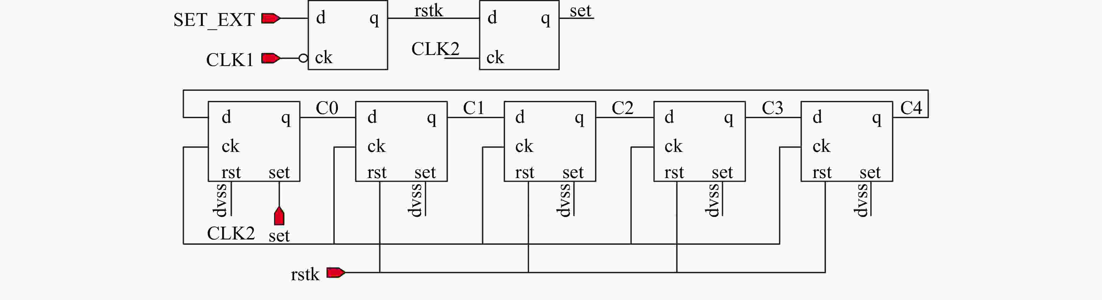
图 2 多相时钟发生器(在线彩图)
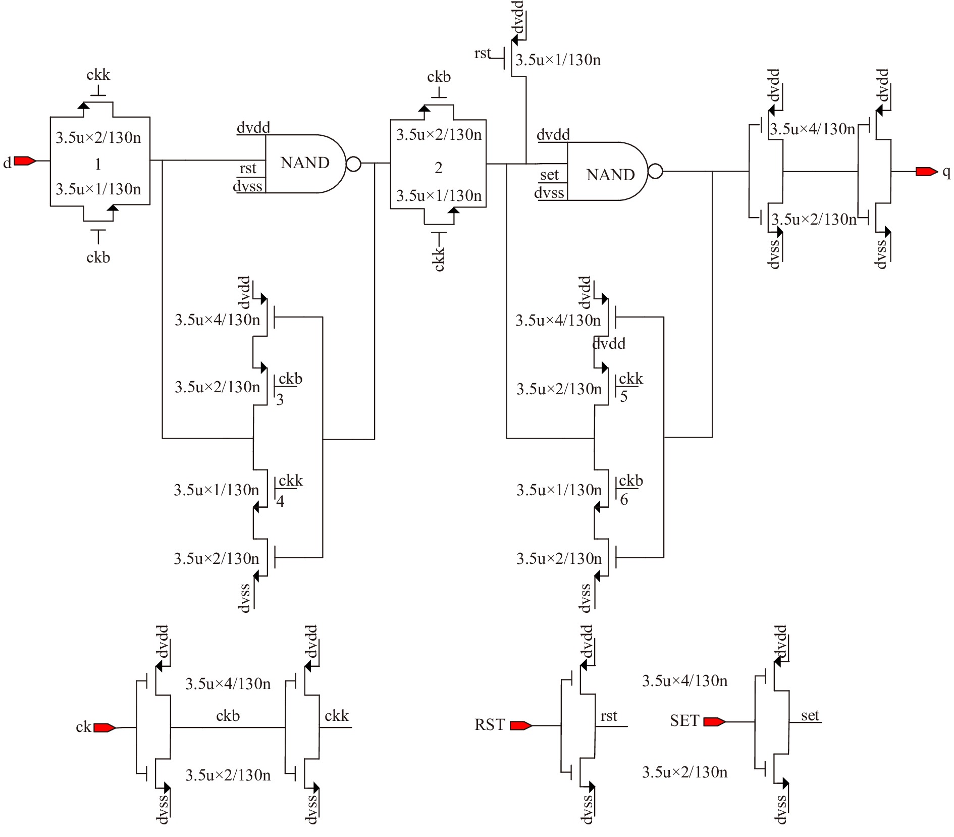
RS型触发器如图3所示,不论输入端d输入高电平信号还是低电平信号,一旦外部复位信号RST有效则输出端q为0,而外部置位信号SET有效则将输出端q置1,这就实现了多相发生器的置位复位功能。同步反相的时钟信号ckk和ckb控制传输门1和传输门2依次循环打开关闭。延迟锁存电路中的MOS管3和MOS管4所加时钟控制信号与传输门2同步,因此可以在传输门2打开时(即传输门1关闭),将延迟锁存电路中的数据信号输入到传输门2,当传输门2关闭时,经过MOS管5和MOS管6延迟的数据信号可以继续输出,从而确保了整个触发器数据输出的延续性。

图 3 RS型(可复位置位型)触发器(在线彩图)
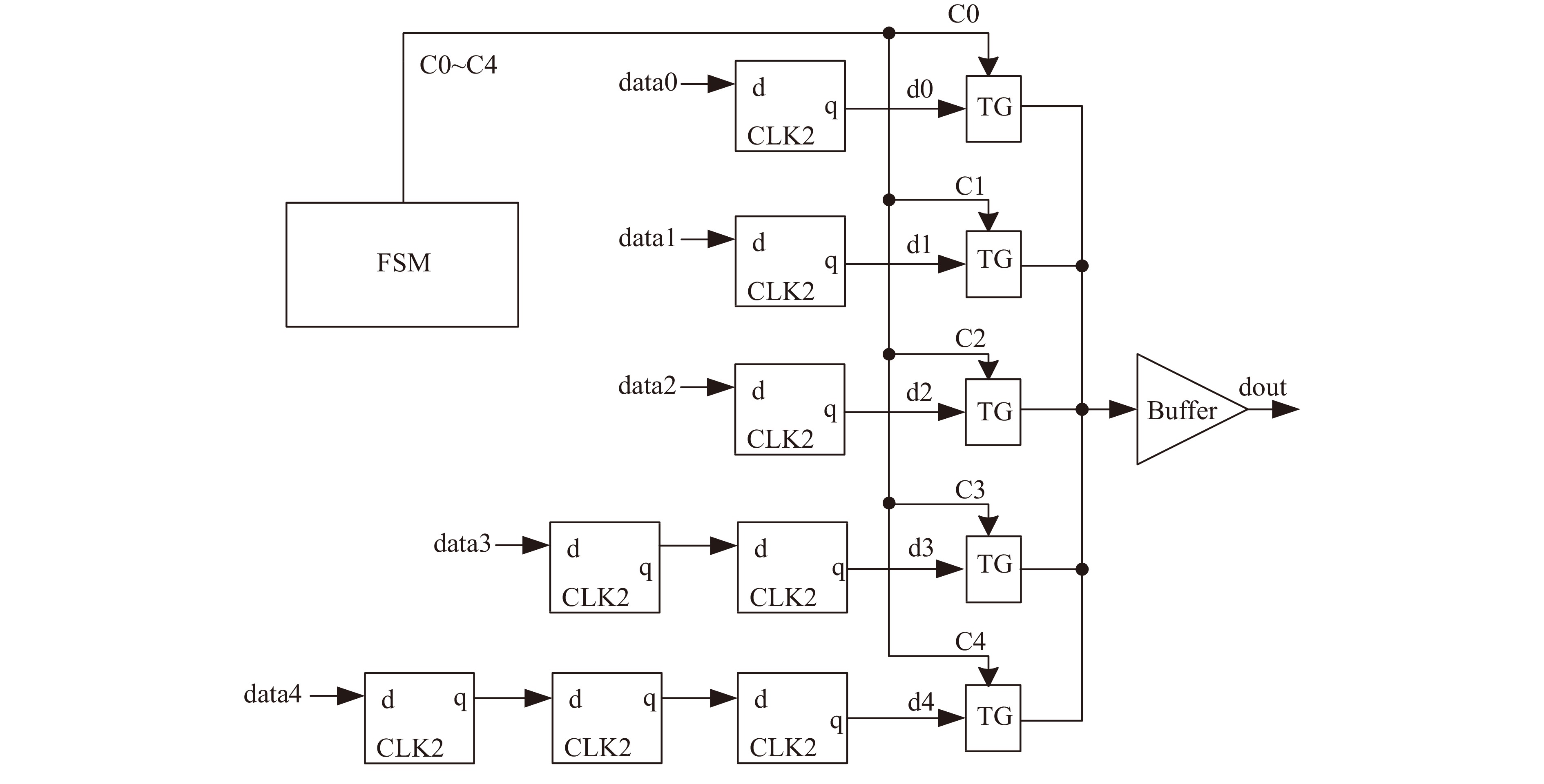
5:1并转串模块的结构如图4所示,主要由5路D触发器组和选通开关序列构成。D触发器组用于将输入数据data0~data4的相位与多相时钟发生器(FSM)提供给选通开关的时钟C0~C4对齐。C0~C4依次打开5路选通开关TG0~TG4,实现从5路250 Mbps的并行数据到1路1.25 Gbps串行数据的转变,5:1转换时序如图5所示。在本设计中,由于FSM总置位信号SET_EXT被片内时钟CLK1和CLK2所同步,因而FSM输出C0~C4与data0~data4存在着固定的相位关系。为了保证FSM输出信号能够正确地依次打开5:1并转串模块的选通开关对输入数据进行采样,五路D触发器组使用了高速时钟CLK2对数据data0~data4的相位进行微调。此外,由于FSM的C4在data4数据结束末期进行采样,可能存在信号完整性问题,因此本设计中每组D触发器的个数不相同,通过高速时钟采样技术,数据data0,data1和data2被延迟800 ps,而data3被延迟1.6 ns,data4被延迟2.4 ns,进而确保C4不在data4数据结束末期进行采样,保证信号完整性[10]。
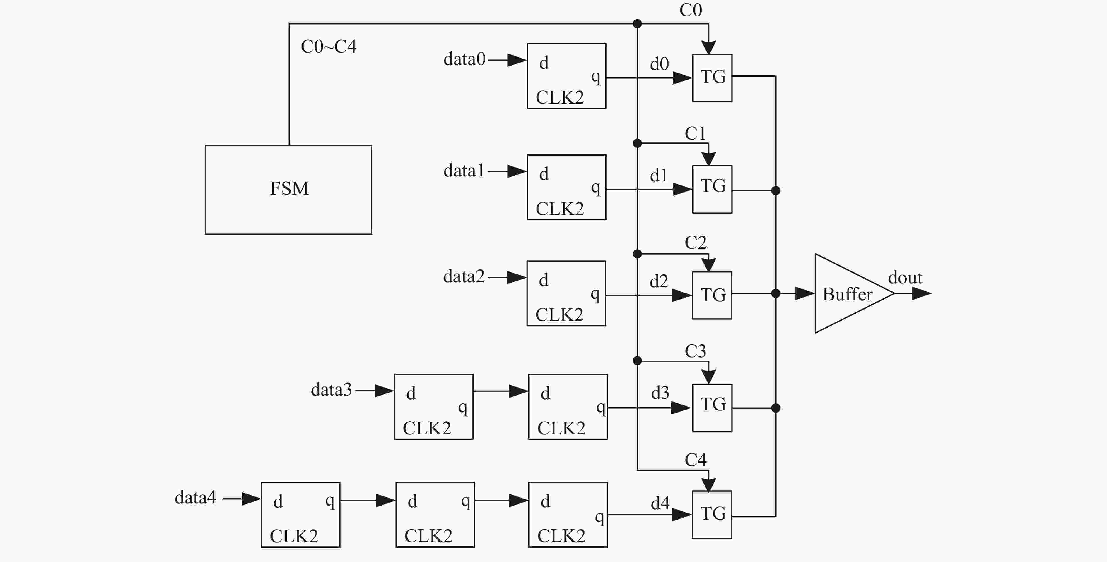
图 4 5:1模块结构图
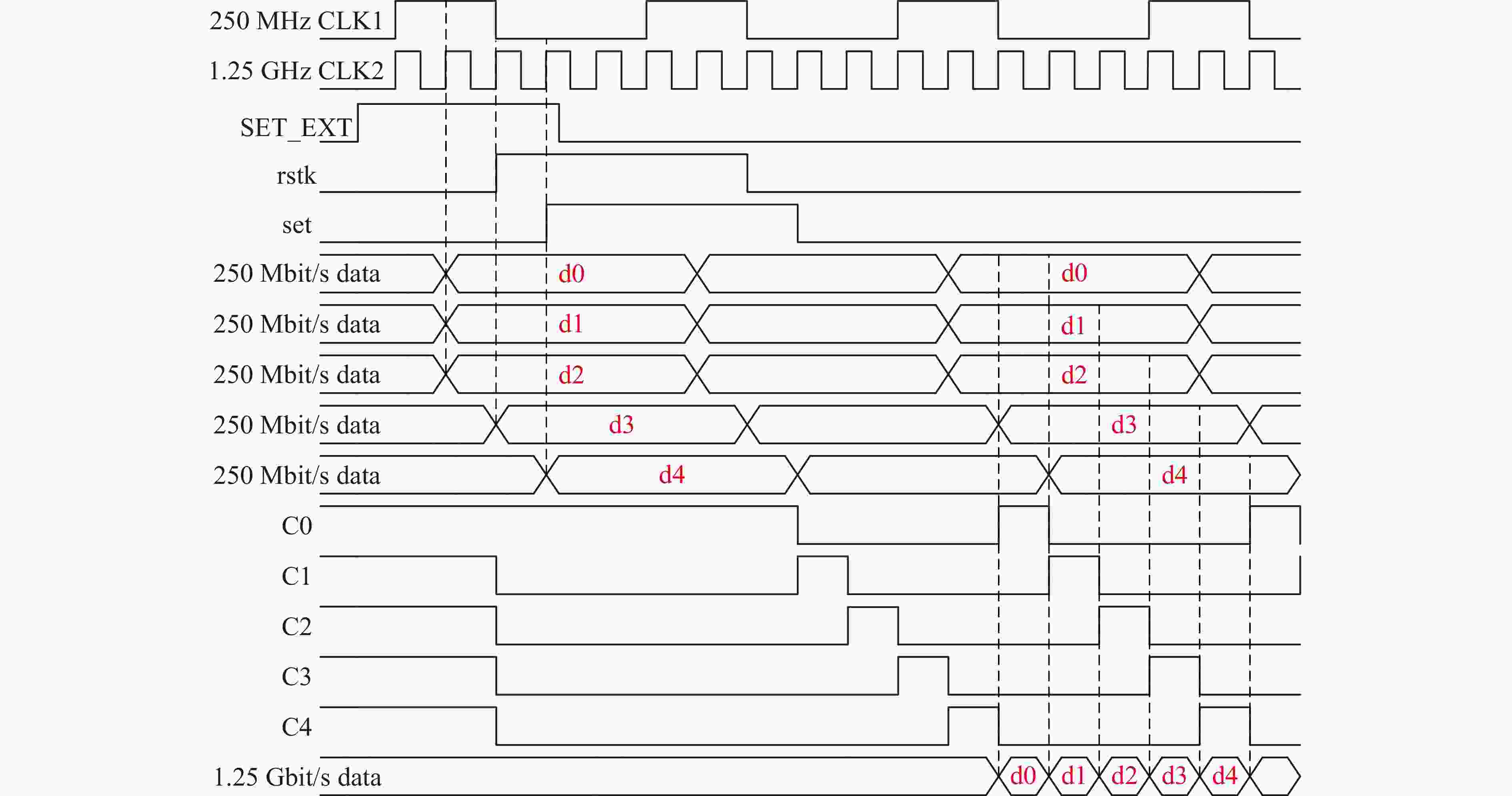
图 5 5:1模块数据时序图(在线彩图)
-
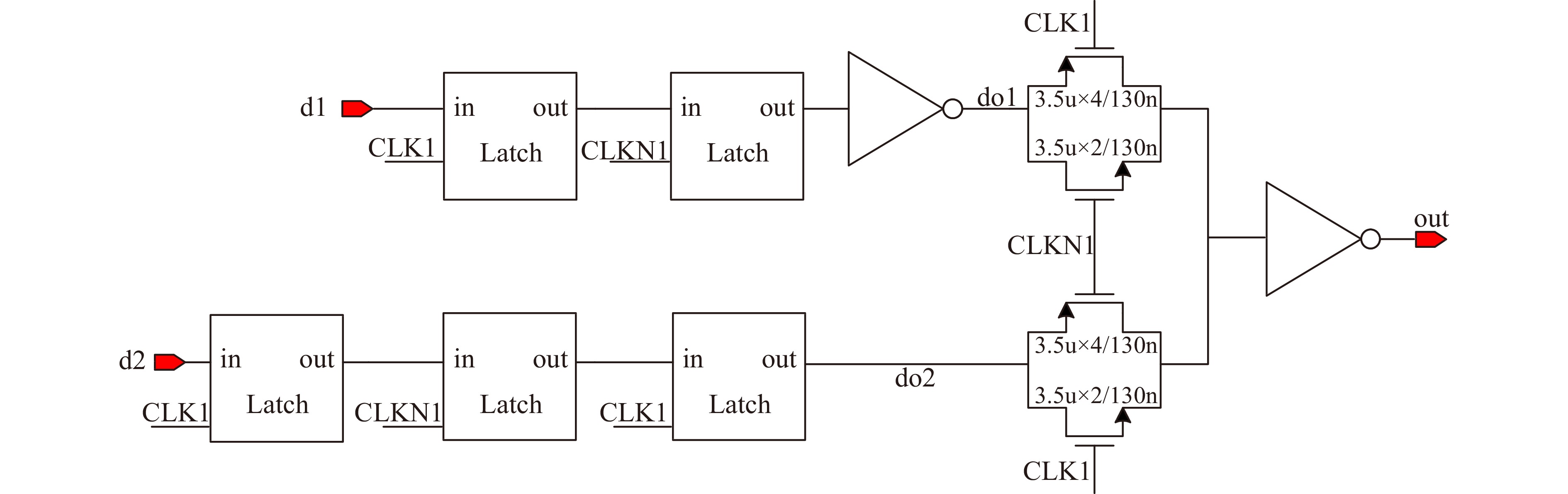
并串转换电路的第二级和第三级均为树型结构的2:1并转串模块,但是由于两级电路在功能与性能上不完全相同,因此两级电路的结构也不完全相同。其中,第二级2:1并转串模块原理图如图6所示,它由两路锁存器序列和选通开关组成。当两路1.25 Gbps串行数据输入至2:1并转串模块的锁存器序列时,由于第二路比第一路多一个锁存器,所以输出的两路数据(do1,do2)固定错开半个CLK1时钟周期(如图7所示)。同步反相的时钟信号CLK1和CLKN1由同一个1.25 GHz时钟信号产生。相位相差半个时钟周期的两路数据do1、do2分别由2个选通开关输出:在CLK1负半周期对第一路输出数据do1中心采样,在CLK1的正半周期对第二路输出数据do2中心采样,最终经过一级反相器后输出一路2.5 Gbps串行数据。
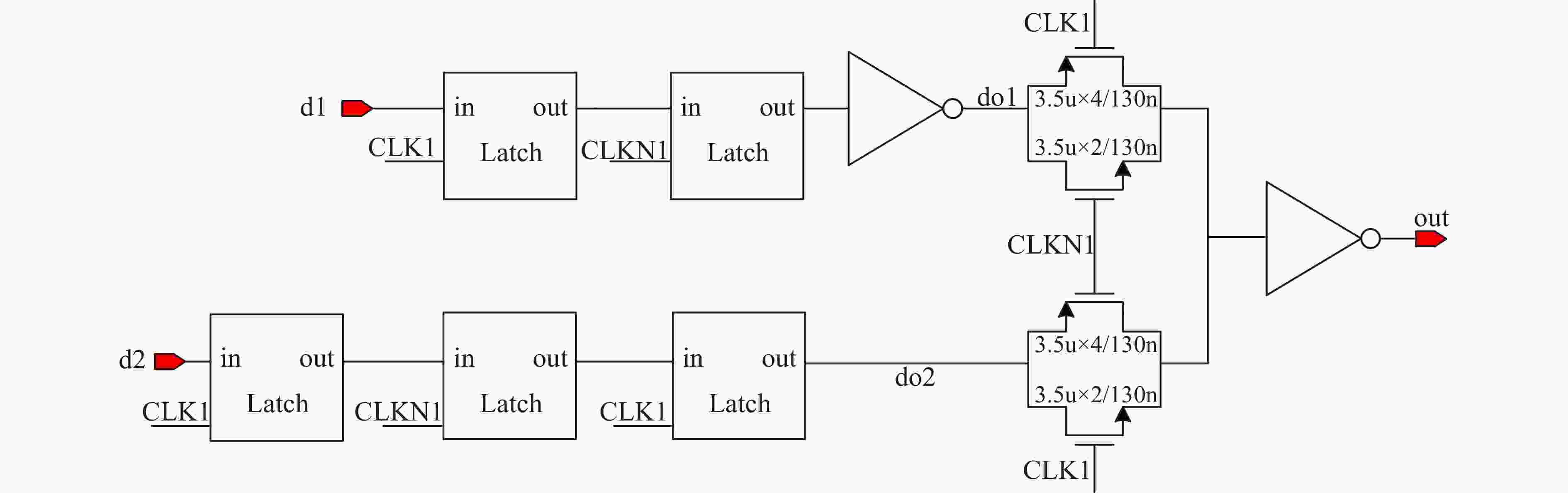
图 6 第二级2:1并转串模块结构图(在线彩图)
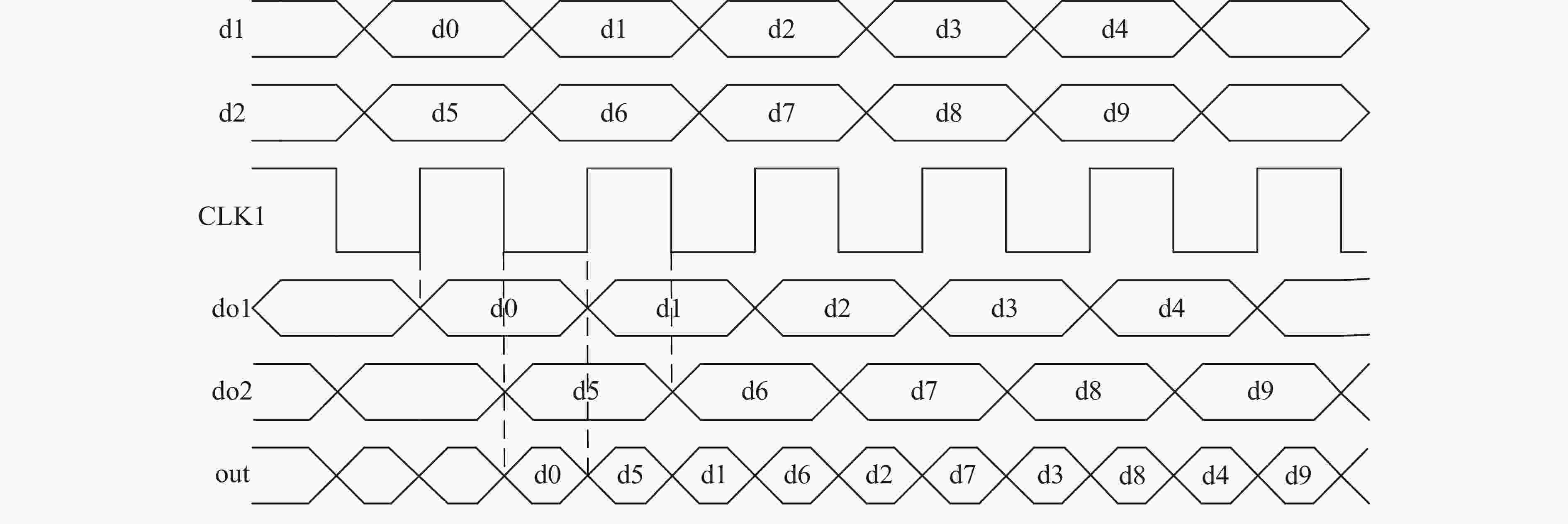
图 7 2:1并转串模块时序图
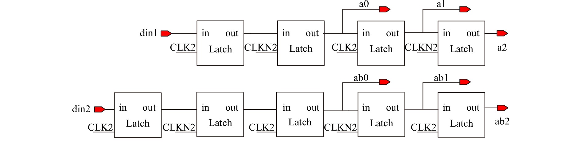
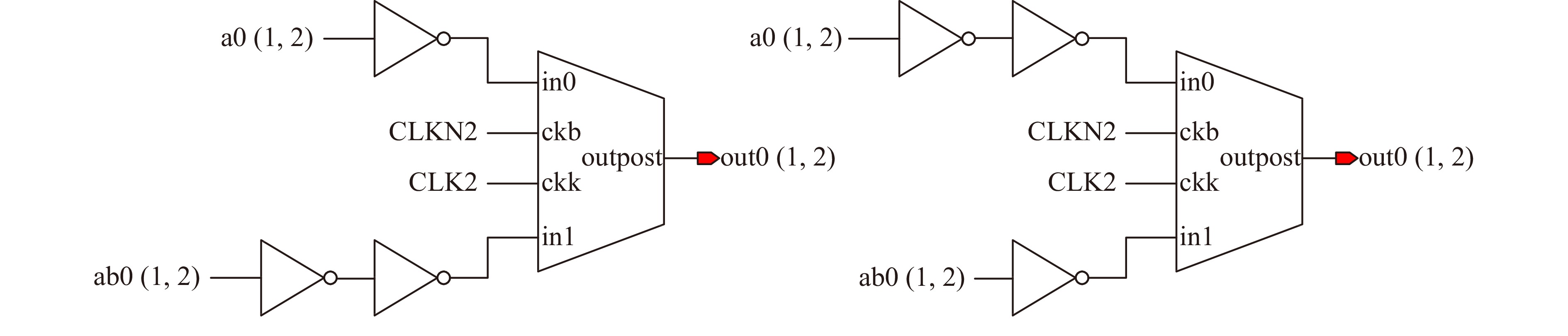
第三级2:1并转串模块的原理图如图8所示,基本原理和第二级2:1并转串模块相同,但是为了保证整个20:1并串转换电路最终的输出信号能够对接全差分驱动器,例如CML驱动器,该级2:1并转串模块也必须设计成差分输出结构。在本设计中,两路输入数据din1和din2通过锁存器与采样时钟对齐之后,引出的6路数据(a0、ab0、a1、ab1、a2、ab2)两两组合分为三组(a0、ab0),(a1、ab1),(a2、ab2),每组数据相差1 bit延时。如图9所示,三组数据分别输入三个差分的二选一MUX电路。其中每组数据中相差半个时钟周期的两路数据分别由2.5 GHz CLK的“1”,“0”信号采样,这样3个二选一电路就会全差分输出3路互相相差1 bit延时的5 Gbps高速串行数据,并且可作为下一级三抽头差分输入型驱动器的输入数据。

图 8 第三级2:1并转串模块结构图(在线彩图)
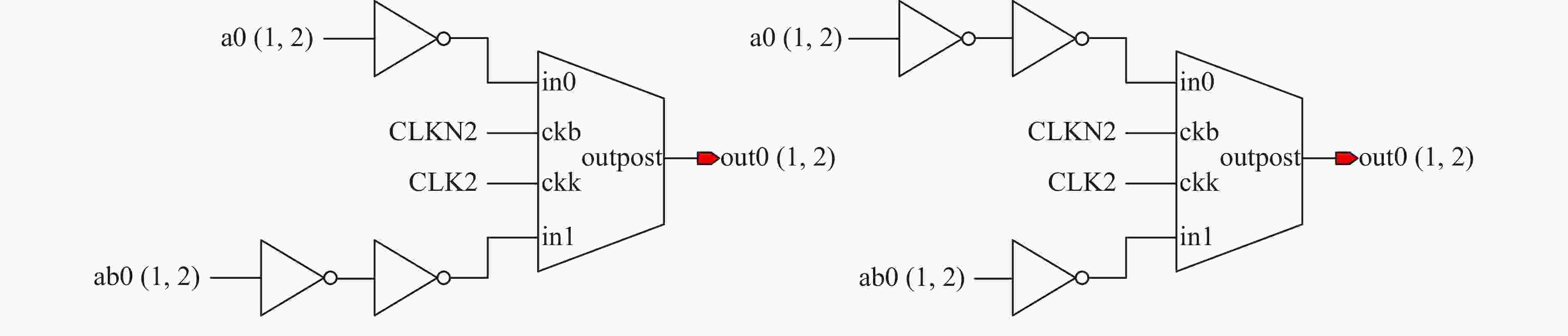
图 9 差分二选一MUX电路结构图(在线彩图)
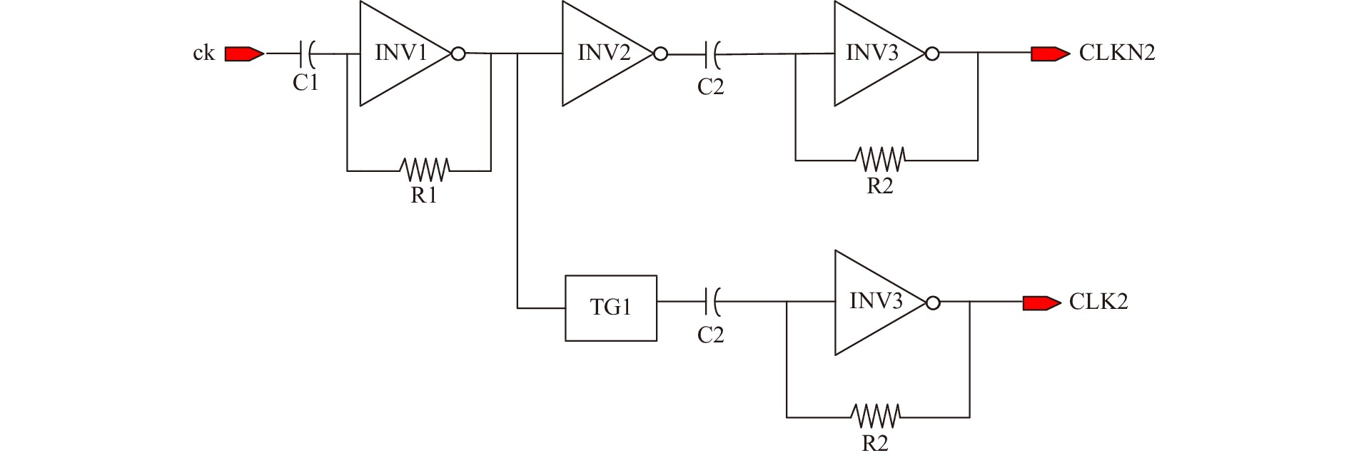
第三级2:1并串转换模块所需的2.5 GHz差分时钟信号CLK2与CLKN2由图10的时钟占空比校准电路(Duty-Cycle Corrector, DCC)产生。为了保证差分时钟在时序上完全一致,INV2和TG的延时需设计成完全相同。由于2:1并串转换模块利用采样时钟的正半周期和负半周期分别对二选一MUX进行选通,即正、负半周期分别对两路数据进行采样。因此,时钟信号的占空比对采样数据的宽度产生直接影响。若时钟占空比不为50%,将导致每比特数据宽度不相同,从而导致眼图两眼宽度不同、抖动变大等问题[11]。

图 10 时钟占空比校准电路(DCC)(在线彩图)
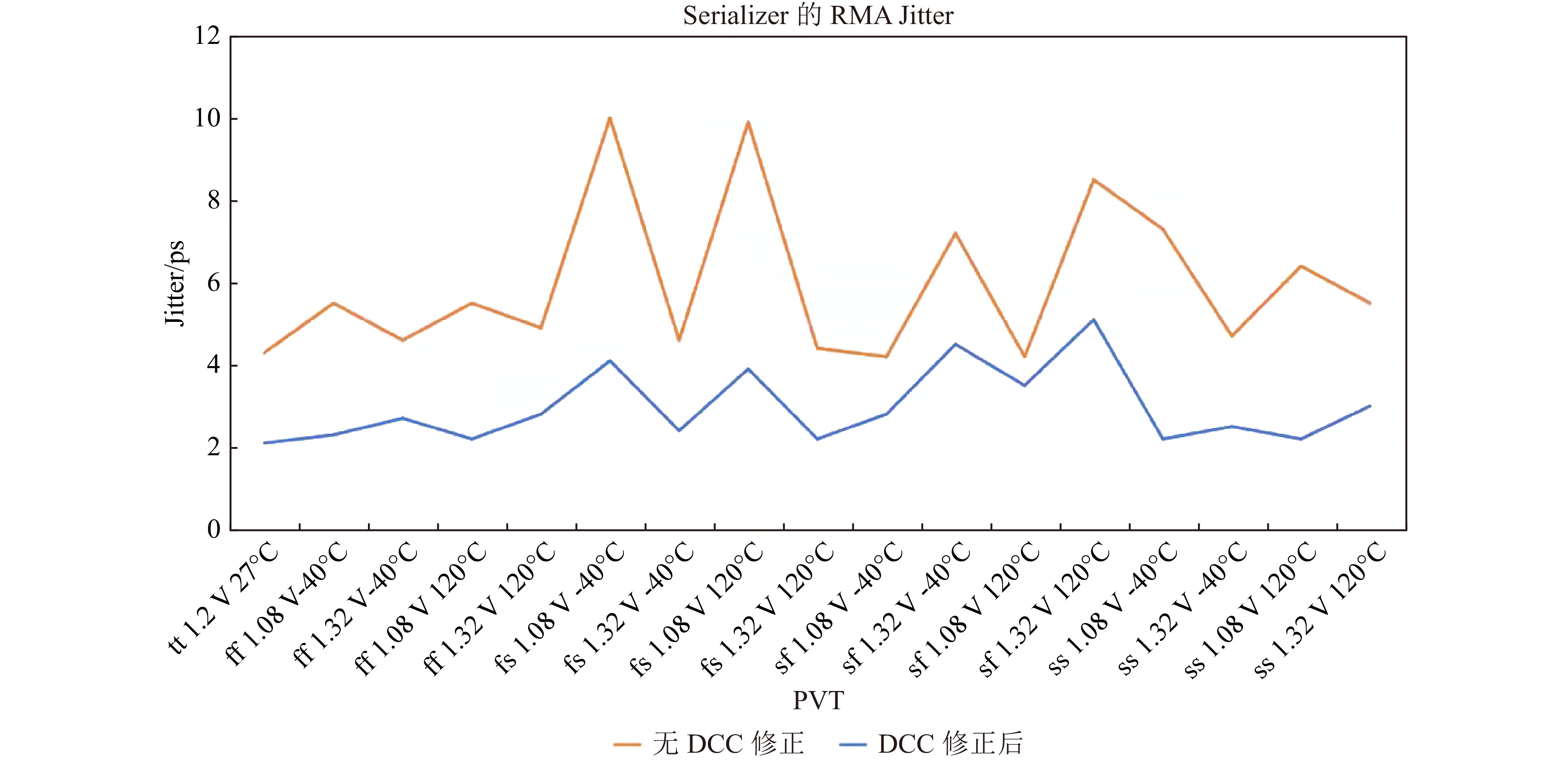
由于反相器提供的时钟信号CLK2和CLKN2的占空比易受PVT(Process、Voltage、Temperature)的影响,为了校准不同PVT下时钟的占空比,本文在时钟驱动电路中加入RC型时钟占空比校准电路来保证产生的时钟信号在所有PVT下占空比接近50%。如图11所示的后仿真结果表明,对时钟驱动电路进行占空比校准后,并串转换器输出数据的RMS jitter(Root Mean Square jitter)得到有效改善。
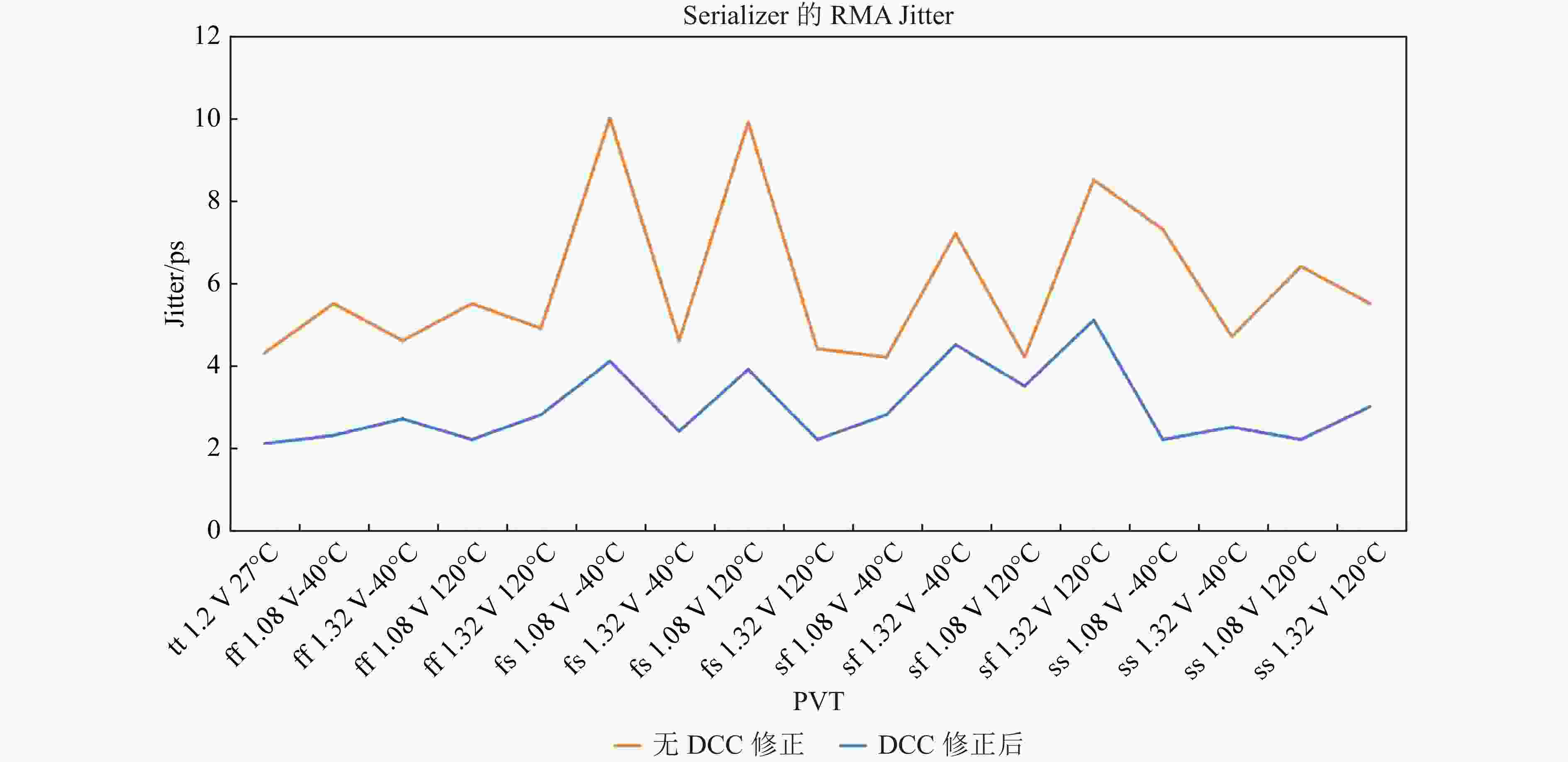
图 11 DCC后仿真结果对比(在线彩图)
-
本设计基于GSMC 130 nm工艺进行版图设计,整体版图如图12所示,其面积为380
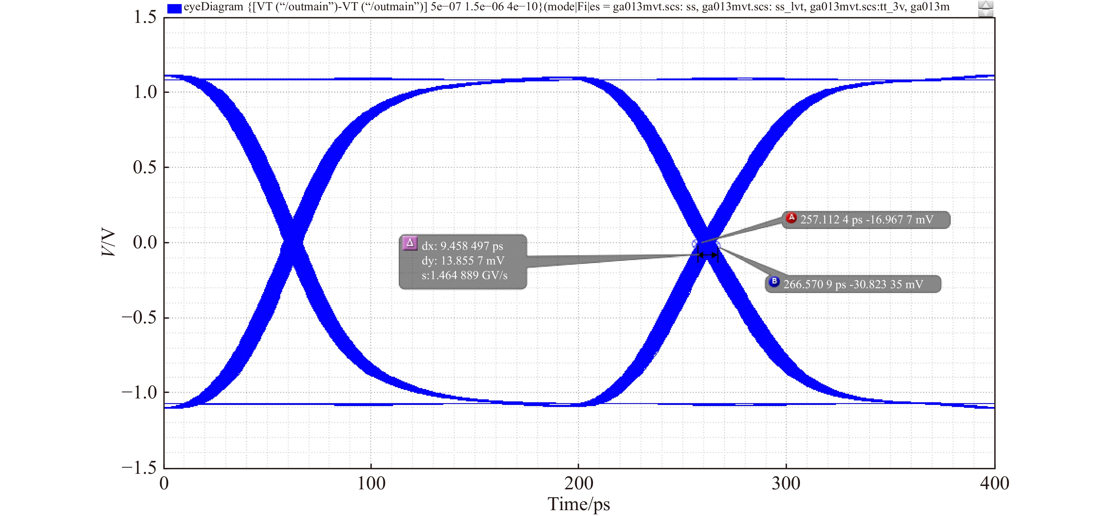
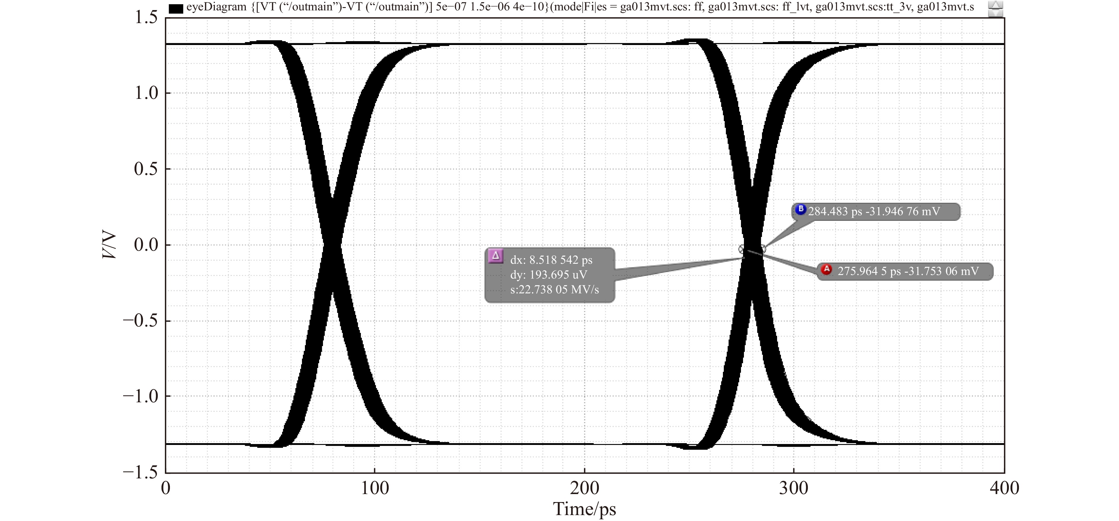
${\mu }\mathrm{m}\times$ 340${\mu }\mathrm{m}$ 。本文对整体版图提取RC寄生参数后按照图13的后仿真测试原理图进行整体后仿真,仿真中加入了瞬态噪声,20路250 Mbps并行数据作为输入。后仿真结果显示,在全工艺角下、−40~100 °C温度范围内、电源电压1.08~1.32 V的条件下输入10 000 bit并行数据,该电路能正确地完成 20:1 并串转换逻辑功能,并输出清晰的5 Gbps数据眼图。如图14所示,在typical(典型值)、电压1.2 V、温度27 °C工艺条件下,输出信号幅度满摆幅时从仿真眼图测量到的总抖动(Total jitter)为 8.34 ps、上升沿为50 ps、下降沿为50 ps、总功耗为39.12 mW。如图15所示,在ff(最快速)、电压1.32 V、温度−40 °C工艺条件下,测量得到总抖动9.46为 ps、上升沿为45 ps、下降沿为45 ps、总功耗40.79 mW。如图16所示,在ss(最慢速)、电压1.08 V、温度100 °C工艺条件下,测量得到总抖动为8.52 ps、上升沿为85 ps、下降沿为82 ps、总功耗为26.89 mW。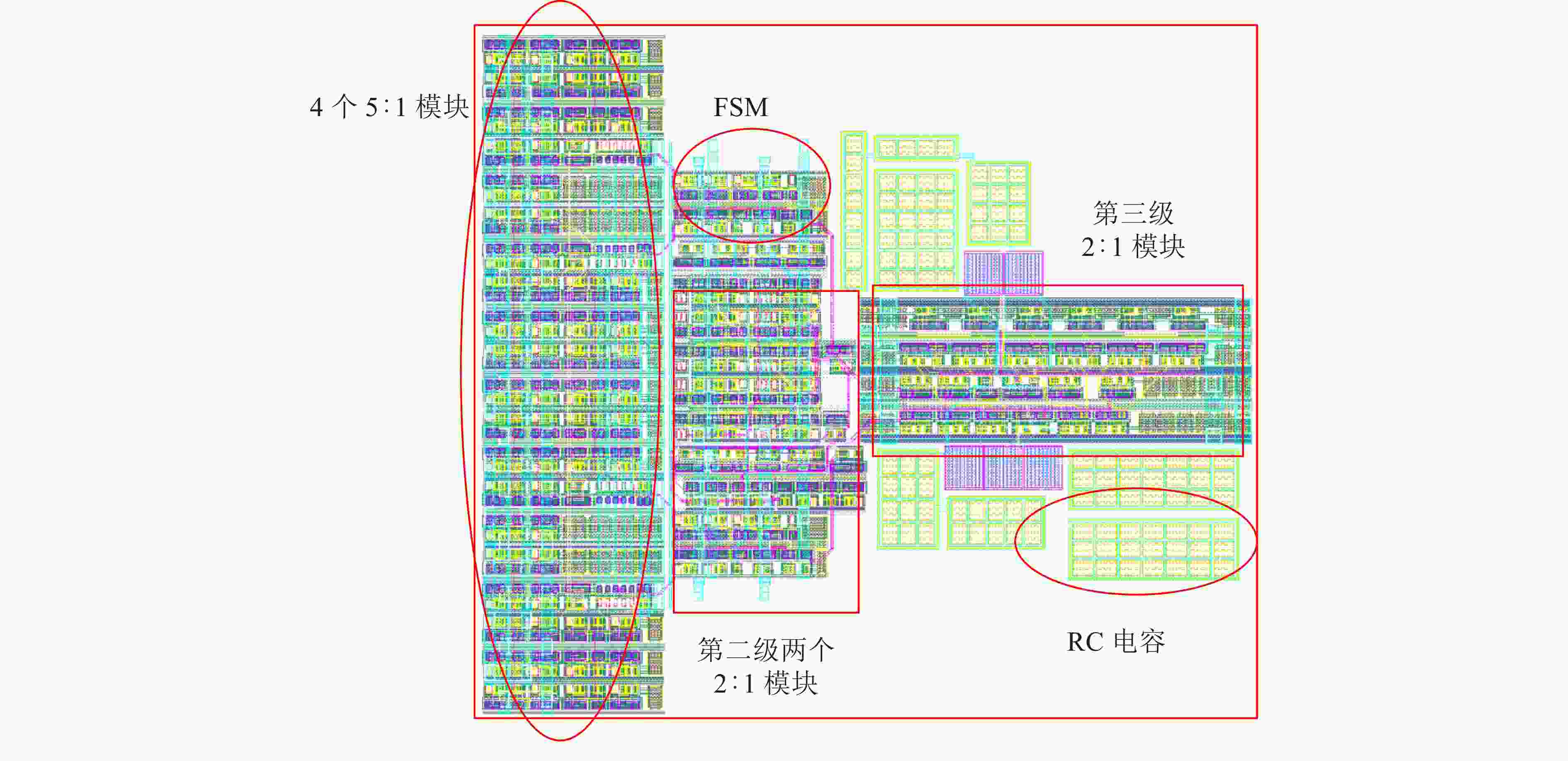
图 12 并串转换模块版图(在线彩图)

图 13 后仿真测试原理图(在线彩图)
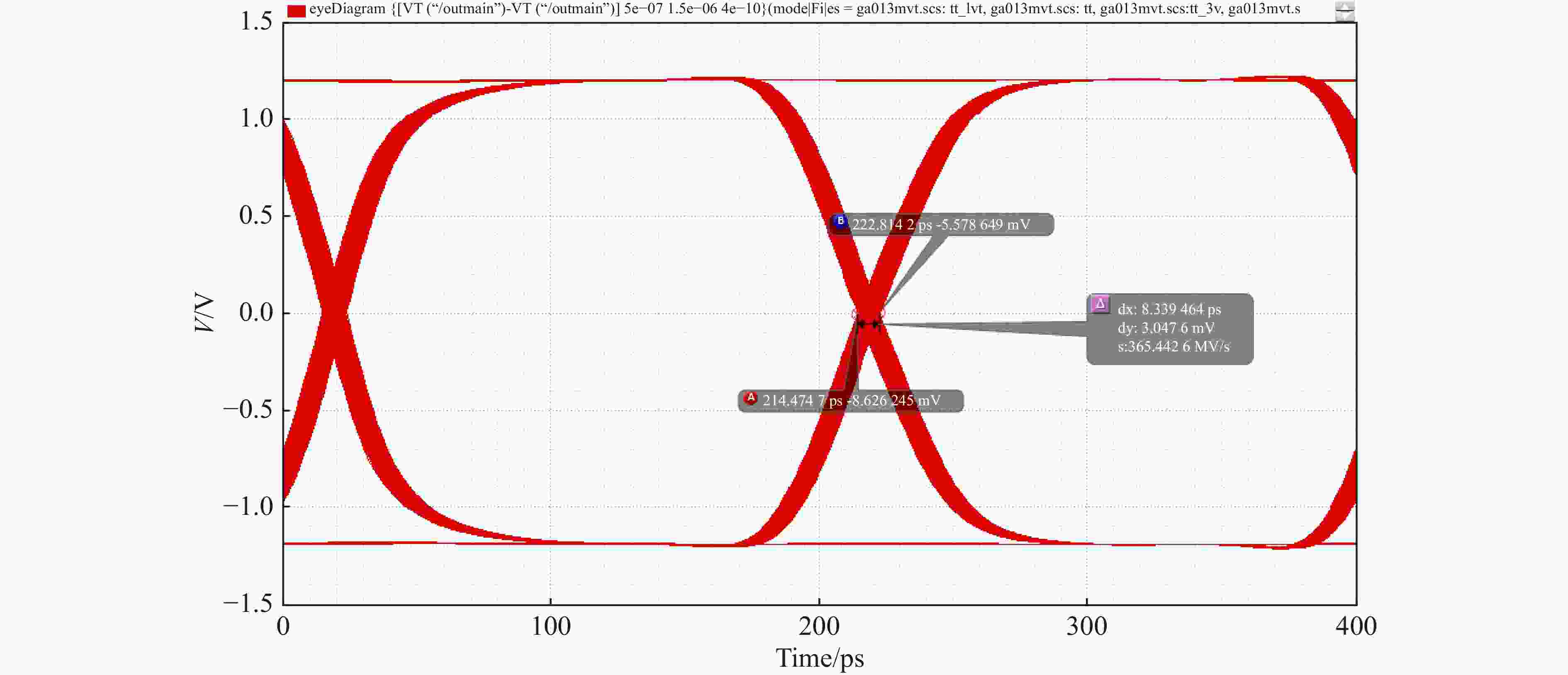
图 14 Typical工艺脚(典型值)、1.2 V供电、27 ℃情况下,芯片后仿真输出眼图(在线彩图)
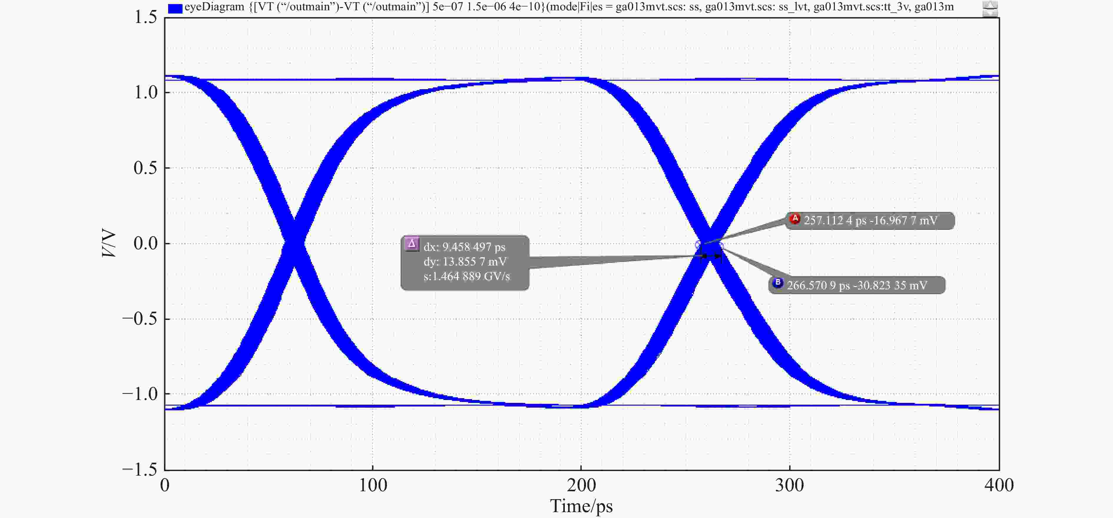
图 15 ff(最快速)工艺脚、1.32 V电压、–40 ℃条件下,后仿真输出眼图(在线彩图)
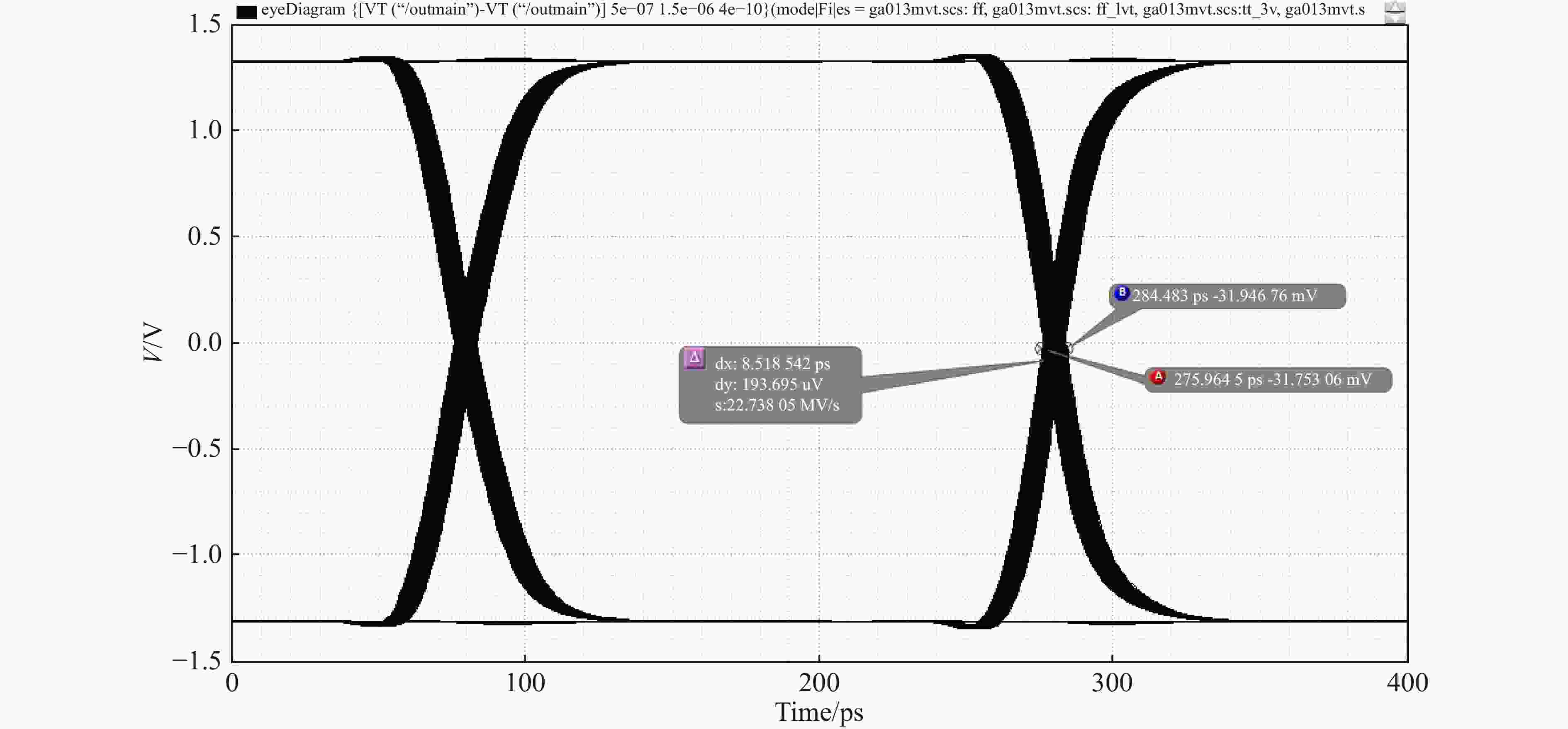
图 16 ss(最慢速)工艺脚、1.08 V电压、100 ℃条件下后仿真输出眼图(在线彩图)
-
本文针对为物理实验装置基于130 nm 国产CMOS工艺研发的5Gbps SERDES芯片的需求,设计了一款20:1的并串转换电路。该电路在整体结构上采用树型结构和多相结构相结合的方式来实现。芯片完整后仿真结果显示,在−40~100 °C温度范围内、工作电压1.08~1.32 V和全工艺角条件下,该电路均可正确完成 20:1 并串转换逻辑功能并输出清晰干净的5 Gbps数据眼图,具有较高速率和低功耗的特点。
-
摘要: 面向全国产化工艺的5 Gbps SerDes(Serializer/DESerializer,串化器/解串器)芯片的需求,设计了其中的20:1 Serializer(并串转换电路)。该并串转换电路基于国产GSMC 130 nm CMOS工艺设计,其内部电路结构设计采用了一级5:1模块和两级2:1模块级联方式,并由多相时钟发生器和分频器提供相应的时钟信号,将20路250 Mbps并行数据转换成1路5 Gbps的高速串行数据进行传输。在温度−40~100 °C、全工艺角环境、电路工作电压在1.08~1.32 V 的条件下,后仿真结果均显示该电路功能正确,能输出完整清晰的5 Gbps数据眼图, 满足设计需求。 其中在27 °C、TT Corner(典型值工艺角)、1.2 V工作电压条件下仿真结果表明该并串转换电路整体总功耗为39.12 mW、总抖动为8.34 ps、输出电压满摆幅为800 mV。Abstract: This paper designs a 20:1 Serializer for a 5 Gbps SerDes (Serializer/DESerializer) ASIC fabricated using China's domestic GSMC 130 nm CMOS process. This Serializer converts the 20-bit 250 Mbps parallel data into 1-bit 5Gbps serial data. It consists of one stage of 5:1 conversion module and two stages of 2:1 conversion module. The clocks are provided by a multi-phase clock generator and a frequency divider. Post-simulations with all process corners, the temperature is from −40 °C to 100 °C and supply voltage is from 1.08 to 1.32 Volt, show this Serializer functions correctly and can generate a clear eye diagram at 5 Gbps, which fulfills the design requirements. Mainly, simulation with the typical process corner, the temperature at 27 °C, and supply voltage at 1.2 Volt show that the total power dissipation is 39.12 mW, the total jitter is 8.34 ps, and the output voltage rail-to-rail is 800 mV.
-
[1] 王伟涛. 8b/10b架构SerDes芯片的设计与实现[D]. 成都: 电子科技大学, 2016(5): 5. WANG Weitao. Design and Implementation of SERDES Chip Based on 8b/10b Architecture[D]. Chengdu:University of Electronic Science and Technology of China, 2016(5): 5. (in Chinese) [2] XIAO L, LI X, GONG D, et al. Journal of Instrumentation, 2016, 11: C02013. doi: 10.1088/1748-0221/11/02/C02013 [3] MOREIRA P, BARON S, BONACINI S, et al. Journal of Instrumentation, 2010, 5: C11022. doi: 10.1088/1748-0221/5/11/C11022 [4] GUETTOUCHE N, BARON S, BIEREIGEL S, et al. Journal of Instrumentation, 2022, 17: C03040(17). doi: 10.1088/1748-0221/17/03/C03040 [5] ZHANG L, CRUDA E M, CHAO C P, et al. Journal of Instrumentation, 2020, 17: C03011. doi: 10.1088/1748-0221/17/03/C03011 [6] 张健忠, 常昌远. 电子与封装, 2007, 7(10): 33. doi: 10.3969/j.issn.1681-1070.2007.10.008 ZHANG Jianzhong, CHANG Changyuan. Electronics & Packaging, 2007, 7(10): 33. (in Chinese) doi: 10.3969/j.issn.1681-1070.2007.10.008 [7] 刘玮, 肖磊, 杨莲兴. 固体电子学研究与进展, 2009, 29(1): 100. doi: 10.3969/j.issn.1000-3819.2009.01.022 LIU Wei, XIAO Lei, YANG Lianxing. Reseerch & Progress of SSE, 2009, 29(1): 100. (in Chinese) doi: 10.3969/j.issn.1000-3819.2009.01.022 [8] 韦龙飞. 多速率SerDes发送模块芯片设计与验证[D]. 成都: 电子科技大学, 2013(6): 15. WEI Longfei. Design and Verification of a Multi-rate Serdes Transmitter[D]. Chengdu:University of Electronic Science and Technology of China, 2013(6): 15. (in Chinese) [9] FUKAISHI M, NAKAMURA K, HEIUCHI H, et al. IEEE Journal of Solid-State Circuits, 2000, 35(11): 1611. doi: 10.1109/4.881206 [10] 孟辰星, 黄光明, 郭迪. 电子与封装, 2020, 20(2): 020303. MENG Chenxing, HUANG Guangming, GUO Di. Electronics & Packaging, 2020, 20(2): 020303. (in Chinese) [11] 伍得阳. 低抖动时钟占空比校准电路的研究与设计[D]. 上海: 复旦大学, 2013(4): 1. WU Deyang. Research and Design of Low Jitter Clock Duty Cycle Calibration Circuit[D]. Shanghai:Fudan University, 2013(4): 1. (in Chinese) -

 点击查看大图
图(16)
计量
- 文章访问数: 801
- HTML全文浏览量: 224
- PDF下载量: 58
- 被引次数: 0


 甘公网安备 62010202000723号